RESEARCH at SNQS
Head of Group: Prof. Dr. Jonathan J. Finley


Growth and Functional Properties of Ultrapure Nanomaterials
 Growth of novel materials and hetero-interfaces:
 Underlying almost all of the science we do at SNQS
is the availability of precise nanostructures created by design using controlled synthesis methods.
We employ high-purity molecular beam epitaxy (MBE) dedicated to III-V compound semiconductors
(group-III arsenides & antimonides), group-III nitrides and, most recently, ultra-pure 2D materials
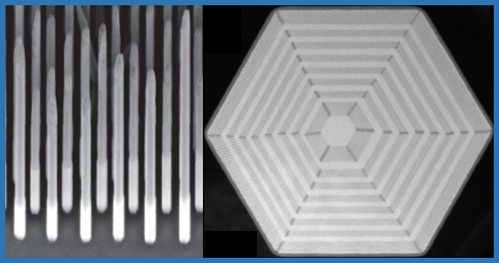
and their heterostructures. Currently, a substantial effort in synthesis is on III-V nanowires (NW),
which offer unique capabilities in heterostructure and crystal phase engineering, as well as site-selective
growth and deterministic incorporation of atomically engineered low-dimensional quantum systems.
More Information?
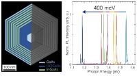 Nanowire Nanolasers:
 Semiconductor lasers promise to have improved performance and novel
properties as their physical size is scaled down to the quantum limit for electrons and photons.
One of the major research directions at SNQS focuses on developing high-performance integrated
(quantum)photonic and optoelectronic devices based on monolithically integrated nanowires (NWs).
Specific examples include NW-based lasers and non-classical single photon emitters based on NW-QD devices.
Hereby, an important task is to explore the optical and photonic responses of the respective systems using
advanced confocal luminescence spectroscopy, where e.g. the effects of the quantized electronic structure,
light-matter interactions, or the coupling of light to on-chip photonic circuits are explored.
More Information?
BACK-TO-TOP
2D-Materials and their Heterostructures
 Spin and Magneto-Optical Phenomena:
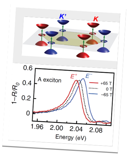
 The optical properties of 2D transition-metal
dichalcogenides (TMDs) such as MoSe2 or WS2, are dominated by excitons, Coulomb-bound particles
comprised of an electron and a hole each of which possesses a spin and valley quantum number.
Because 2D materials are so thin materials directly adjacent to the TMD layer can influence spin and
magneto-optical properties. SNQS researchers are interested in questions like: What are the fundamental
spin- and excitonic-excitations in TMDs? How does the dielectric / magnetic / topological environment
influence the excitons?
 Localized excitons in 2D-materials:
 Localized excitons in 2D materials have shown to be
sources of non-classical light. SNQS researchers follow three avenues for exciton localization:
(i) dielectric engineering, (ii) strain-induced exciton localization and (iii) site-selective
generation of native defects via He-ion irradiation. Our goals are to understand the mechanisms of
localization for couple light from such localized emitters into photonic structures and explore
interesting phases of interacting excitations in defined trapping potentials. Here, we work closely
with the Ultrafast Optoelectronics group led by
Alexander Holleitner at WSI, the
Experimental Semiconductor Physics group led by
Ian Sharp and the
Photonic Quantum Engineering group at
TUM-ECE led by
Kai Müller.
More Information?
 Novel heterostructures with 2D perovskites:
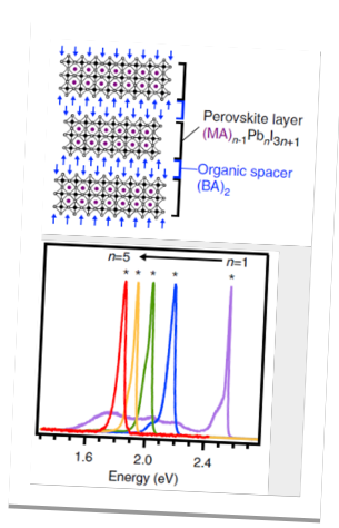
 Similar to conventional III-V semiconductor
superlattices, Ruddlesden-Popper halide perovskites are quantum well-like structures formed by
two-dimensional layers of halide perovskites semiconductors, separated by organic spacer layers.
This layered structure can be tuned by varying the perovskite layer thickness and the composition of
the organic layer. Although efficient opto-electronic devices were made from such materials,
fundamental questions concerning the nature of optical resonances remain. SNQS researchers strive to
understand how the optical properties of these fascinating materials can be controlled, especially
when they are combined with other 2D-materials.
More Information?
BACK-TO-TOP
Quantum Optics of Solids
Quantum optics and spin-photon interfaces in single and coupled-QDs: SNQS researchers
investigate quantum optical methods to prepare, manipulate and readout optically active quantum
spin-states in semiconductor QDs. Due to their strong optical transitions with almost transform-limited
linewidth, QDs are ideal prototypes for solid-state quantum emitters. Among our current experiments are
resonance fluorescence investigations of quantum optical properties of QDs, investigations of the
complex
dynamics of single electron and hole spins confined to QDs and the use of QD-molecules for
solid-state quantum repeaters. SNQS works closely with the
Photonic Quantum Engineering group at
TUM-ECE led by
Kai Müller.
More Information?
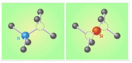 Diamond Quantum Optics:
 Diamond is well known to host interesting spin-centers with strong
optical activity and coherent spin dynamics up to elevated temperatures. Besides the well-studied
NV-center, other color centers such as SiV, GeV and SnV have recently moved into focus by virtue of
their excellent quantum optical properties at low-temperatures. However, diamond is difficult to
nano-pattern to enhance the light-matter coupling towards the deterministic limit. Here, SNQS
researchers work on patterning diamond containing quantum emitters and their use for the generation
of photonic cluster states for quantum communication. SNQS works closely with the
Photonic Quantum Engineering group and the
Chair of Theoretical Information Technology
at TUM-ECE.
More Information?
BACK-TO-TOP
Quantum Photonics
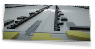
 Photonic crystal nanostructures:
 Photonic crystals consist of regularly patterned arrays of
materials with different dielectric constants, giving rise to a band structure for light.
In particular, one and two-dimensional photonic crystal nanostructures provide a platform for
integrated quantum-photonics including nano-cavities, waveguides, splitters and interferometers
and allow the exploration of chiral and non-commensurate states of light. We study
light-matter-interactions between discrete quantum emitters and tailored optical modes in
photonic nanomaterials with topics linking fundamental quantum optics to sensing and metrology.
More Information?
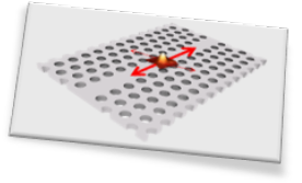
 Optics at the nanoscale:
 Focusing electromagnetic fields form far field to nanoscale
dimensions is one of the central research goals in nanooptics. While conventional diffractive
optics are limited by the Abbé diffraction limit, metal optics offers routes to concentrate
far-field radiation into volumes of only a few cubic nanometers and as a result of that
give rise to extraordinarily enhanced electromagnetic near-fields.
More Information?
BACK-TO-TOP
Quantum Sensing and Metrology
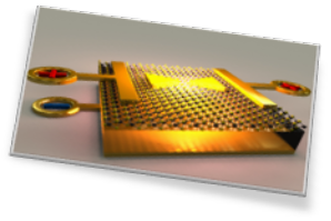
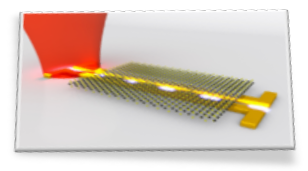
 On-chip single photon detectors:
 Patterned superconducting thin films have recently been
exploited for realizing high-efficiency, ultra-fast and broadband photon detectors with the capability
to detect light down to the single photon level. We are working closely with the company
Kiutra GmbH
and the group of
Kai Müller to realize superconducting
nanowire single photon detectors for emergent quantum technologies.
More Information?
Optics at the nanoscale: Focusing electromagnetic fields form far field to nanoscale
dimensions is one of the central research goals in nanooptics. While conventional diffractive
optics are limited by the Abbé diffraction limit, metal optics offers routes to concentrate
far-field radiation into volumes of only a few cubic nanometers and as a result of that
give rise to extraordinarily enhanced electromagnetic near-fields.
More Information?
BACK-TO-TOP


 Walter Schottky Institut