|
Functional Interfaces
|
|
"Controlling how materials interact with complex environments enables advances in fields ranging from biological and chemical sensing to artificial photosynthesis. In the WSI, we create hybrid organic/inorganic interfaces, semiconductor/electrolyte junctions, and engineered solid state heterostructures to achieve specific functionality and explore interactions where solid materials meet their surroundings."
|
|
Current Work
|
|
 |
|
|
|
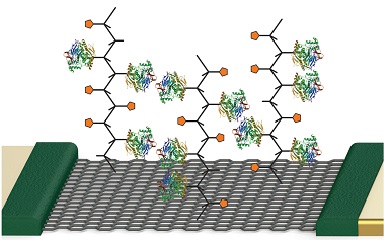
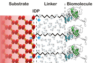
Combining the ultimate precision of molecular systems with the broadly tunable (opto)electronic properties of inorganic semiconductors allows formation of hybrid systems with tailored functionality. In this context, we explore the properties of a range of organic/inorganic and biological/inorganic assemblies with function tailored for selective catalysis, sensing, and nanoscale electronics.
Stutzmann
|
|
|
 |
|
|
|
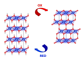
Catalysts with low kinetic overpotentials, high chemical selectivity, and long-term operational stability against both deactivation and degradation are required for water splitting and fuel formation reactions. Physical and chemical deposition approaches are used to form compound catalysts in forms ranging from clusters, to particles, to thin films. A range of advanced spectroscopic, electrochemical, and analytical tools are used to correlate material and chemical transformations with key catalytic properties.
Sharp
Stutzmann
Wurstbauer
|
|
|
 |
|
|
|
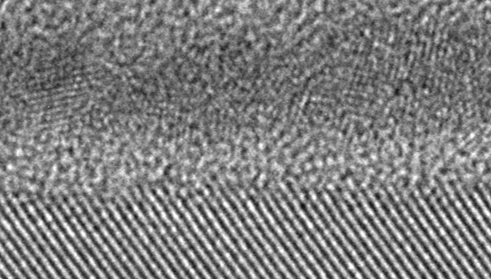
Efficient, selective, and robust photochemical systems require precise control over light interactions with matter, charge carrier separation and transport, and competing chemical pathways. The assembly of solid/solid heterostructures via advanced deposition and nanofabrication methods provides opportunity to balance competing properties and is used to achieve new combinations of physical and chemical functionality.
Sharp
Stutzmann
|
|
|
 |
|
|
|
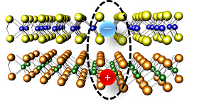
2D materials can be stacked on top of each other forming so-called 2D heterostacks. The latter are particularly fascinating for excess charge carrier transport, because photogenerated electrons and holes in different layers can form so-called indirect or dipolar excitons.
Finley
Holleitner
Kaniber
Wurstbauer
|
|
|
|

 Walter Schottky Institut