An Introduction to Semiconductors
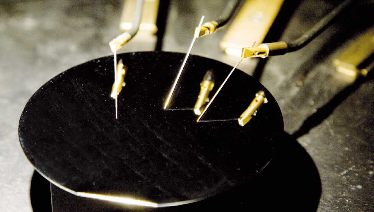
A modern version of Ferdinand Braun's experiment
On the 14th of November, 1876, the high school teacher Ferdinand Braun gave a presentation entitled “Experiments concerning deviations from Ohm’s Law in metallic conductors” in front of the illustrious Naturforschende Gesellschaft zu Leipzig. Neither Mr. Braun nor his critical audience were aware of the fact that they were just witnessing the birth of Semiconductor Physics. Indeed, what Ferdinand Braun had discovered by a long series of meticulous experiments, at first sight did not appear too exciting: if one equipped a solid crystal with two metallic contacts and applied an electrical voltage, two basic kinds of behavior could be observed. Either no measurable electrical current passed through the crystal. Then this crystal obviously was an electrical insulator and, therefore, was no longer of interest for further investigation of its electrical properties. Or, for the second type of crystals, a sizeable current could be measured. Then this crystal was a metallic conductor and obeyed Ohm’s Law. If one doubled the applied voltage, also the observed current was doubled. And if one inverted the electrical voltage applied to the two contacts, also the current was inverted. At least, that was the way it used to be until 1876...
The deviations from Ohm’s Law, which Ferdinand Braun reported to the Natural Society at Leipzig, were quite strange, indeed. Instead of using large electrical contacts, Mr. Braun had performed some of his experiments with very fine contact needles. In some crystals he then had observed an electrical current as in a usual conductor, but when he inverted the applied voltage, the current disappeared and the crystal apparently had converted to an insulator. Similarly unexpected was what happened when Braun changed the magnitude of the applied voltage. Then for these strange crystals the current increased much more strongly than allowed by Ohm’s Law.
What Ferdinand Braun had discovered was the first semiconductor device ever: a rectifying diode, which could transform alternating current into direct current, and many years later actually was used in the form of point contact diodes in radio receivers or radar units. Unfortunately, the reason for this strange behavior of his crystals remained entirely mysterious to Ferdinand Braun. The scientific explanation of this phenomenon only was given much later in 1939 by Walter Schottky, who at that time developed a theory for the electronic properties of semiconductor/metal-interfaces. Honoring this work, rectifying metal/semiconductor contacts now are known as Schottky diodes. As for Ferdinand Braun, he received the Nobel Prize for Physics in 1909 and today mainly is remembered for the invention of the cathode ray tube. As a matter of fact, due to the development of vacuum tubes, solid state electronics did not gain any practical importance until the first transistor was built by Bardeen, Brattain, and Shockley in 1947. Since then, however, solid state electronics based on semiconductor devices has revolutionized our world, which no longer can be imagined without this.
So what actually are semiconductors, what makes them so different from metallic conductors, and why are they so interesting for many applications? The scientific answer to these questions and the development of new semiconductor materials and devices is what semiconductor physics and technology is all about. It takes many years of intensive studies to master the basics of this important part of solid state physics. Here, we will try to convey the most important concepts concerning the unique properties of semiconductors with the help of a simple analogy.
In a regular periodic crystal lattice, electrons as the carriers of electrical current are not allowed to move around freely. Instead, they have to obey certain rules enforced by quantum mechanics. As a consequence, electrons have to occupy so-called “energy bands” which are separated from each other by small or large “band gaps”. This situation can be compared to a two-storey building consisting of a ground floor and a first floor. In the language of solid state physics, these two storeys are called “valence band” and “conduction band”, respectively. Both floors are covered by a well-ordered array of quadratic tiles, representing the periodic lattice of atoms in a semiconductor crystal. The movement of electrons in a crystal is then analogous to the movement of inhabitants in our building, whose most important purpose it is to transport “charge” from one end of the building to the other end. The inhabitants of our “semiconductor house” have to obey one additional important rule: at no time more than one inhabitant is allowed to occupy the space of a given tile! In the same way, electrons in a solid crystal have to obey the quantum-mechanical “exclusion principle” formulated by the famous physicist Wolfgang Pauli.

Occupation of the valence band (ground floor) and the conduction band (first floor) of a semiconductor with electrons (inhabitants).
Now that the blueprints of our semiconductor building and the basic rules for its inhabitants have been defined, let us start to occupy this building with people. At first, all inhabitants can be accommodated on the ground floor, where they can move around more or less freely and transport their cargo across the building. This leads to a steady increase of the amount of cargo transported through the building, until the occupancy of the ground floor has increased so much that the inhabitants start to hinder one another on their way. Eventually, the stream of cargo will come to a complete stop, once all tiles in the ground floor are occupied by an inhabitant, so that nobody is able to move any more. Further inhabitants can only occupy the first floor, where they again have sufficient room to move about. As a consequence, the overall cargo stream through the building will again start to increase, reach a maximum, and eventually come to an end when also the first floor is fully occuppied.
The fate of electrons in solids is quite similar to what happens to the inhabitants of our semiconductor building. In particular, it is easy to understand why both, electrical conductors as well as insulators exist in nature. Crystals in which energy bands are only partially filled will belong to the group of electrical conductors, since their electrons can move more or less freely through the crystal lattice. If, on the other hand, all energy bands are fully occupied or completely empty, no electrical current can pass through the crystal at all and we are dealing with an electrical insulator. Which situation will be encountered for a given solid crystal depends on how many electrons per atom are available to occupy the energy bands of the crystal. For example, almost all metals are very good electrical conductors due to a half-filled conduction band, whereas metal oxides very often are good insulators with a completely filled valence band and an empty conduction band.
Now, how do semiconductors fit into this picture? As already suggested by their name, semiconductors are solids which are able to pass an electrical current much better than insulators, but at the same time not as efficiently as an electrical conductor. Obviously, semiconductors are solids in which for one reason or the other a few of the many tiles on the ground floor remain empty or a few of the conduction band tiles are occupied, or both. This particular constellation can be achieved via three routes, all of which are of fundamental importance in semiconductor physics and, thus, will be treated in more detail in the following.

Model of a p-type semiconductor with acceptor atoms

N-type semiconductor with additional electrons donated to the conduction band by donor atoms
The starting point of our discussion will be the situation of an electrical insulator, where all tiles in the ground floor are occupied by exactly one inhabitant and all tiles in the first floor are empty. Thus, no charge transport can occur. To change this state of affairs, which is very unfavorable for device applications, semiconductor physicists have developed the concept of “doping”. Contrary to the very negative image in sports, doping in semiconductors can be used to exactly pre-determine the electrical conductivity of a given device by addition of a precisely calculated amount of impurity atoms. In the analogue of our semiconductor building, doping can be achieved by adding special tiles with the following properties. As a first example, so-called “acceptor tiles” can be added to the ground floor. These acceptor tiles have the unpleasant property of swallowing exactly one inhabitant of the fully occupied ground floor, thus creating a “hole” in the overall occupancy. This allows the other inhabitants of the ground floor to move again. The hole created by the acceptor-tiles also will move at the same time, however in the opposite direction as compared to the inhabitants. In the same way, acceptor atoms incorporated into a semiconductor crystal will create a hole in the occupancy of the valence band, which will act as a “missing electron” and, thus, as a positively charged particle in electrical transport. Therefore, doping of a semiconductor crystal with acceptor atoms is referred to as “p-type” doping (“p” as in positive). The second possibility to induce controlled electrical conduction in an insulator is the doping with donor impurities. In our semiconductor building, such “donor tiles” bring along one additional inhabitant, who has to occupy a free tile in the first floor, since all tiles of the ground floor are already occupied. Accordingly, donor atoms added to a semiconductor crystal will provide additional electrons in the conduction band, which contribute to electronic charge transport in the expected way (“n-type” doping by additional negatively charged electrons).
In summary, it is indeed the possibility of doping with additional donor or acceptor atoms which distinguishes semiconductors from insulators or conductors as a third class of materials. Conductors will always pass electrical current with little resistance and independent of chemical details, no matter what. In the same way, insulators will always block electrical current. In contrast, semiconductors will either behave more like an insulator or more like a metal, depending on the level of doping. This provides semiconductors with the unique property to rectify, switch, or amplify electrical signals and, thus, to manipulate electrical current as it passes through the semiconductor crystal.

Undoped semiconductor with thermally excited electrons and holes
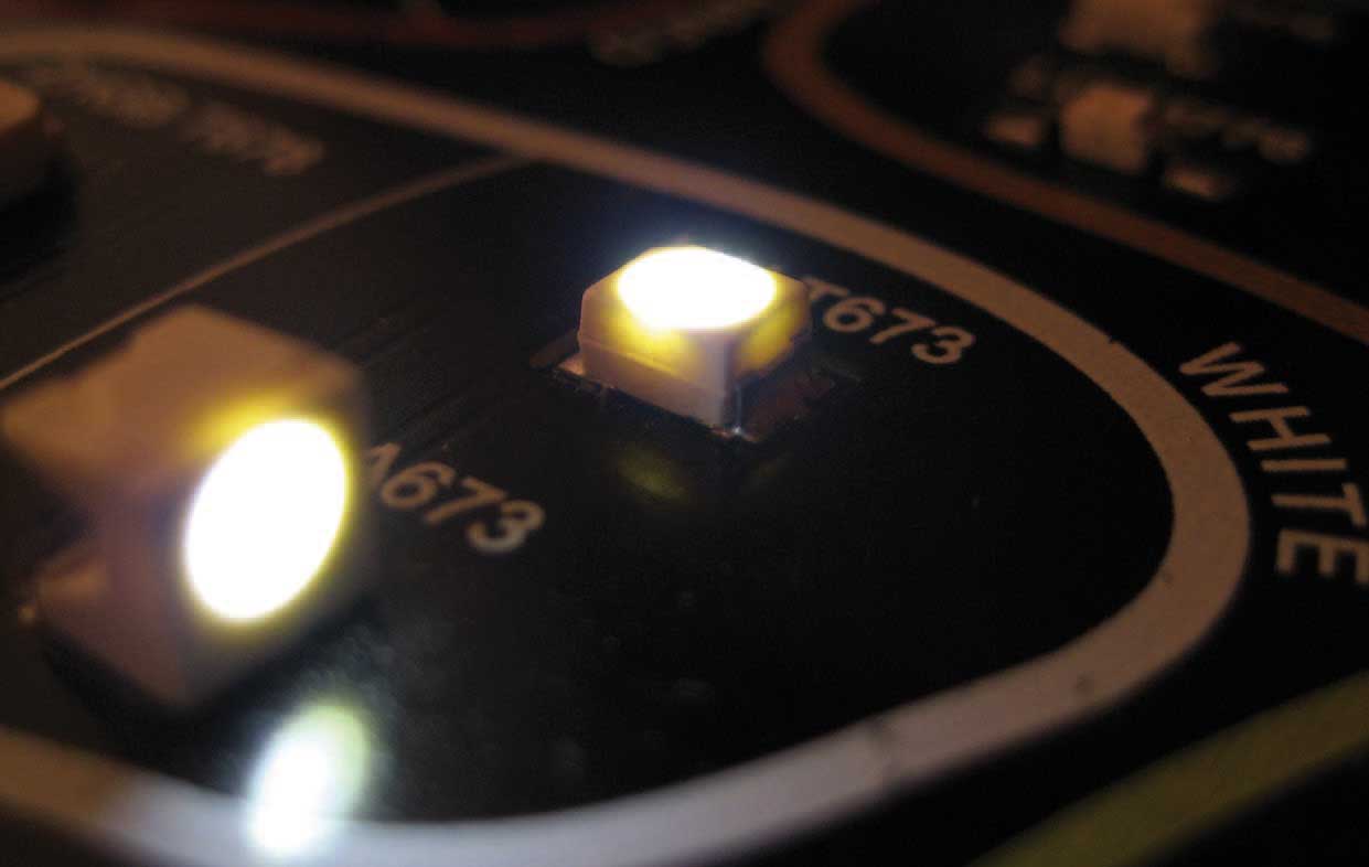
There is yet another way to produce additional holes in the valence band or electrons in the conduction band of a semiconductor without doping, namely by providing external energy in the form of heat or light. We all know from our own experience that it takes energy to walk up the stairs from the ground floor to the first floor. The same holds for the electrons in a semiconductor: electrons in the conduction band (first floor) have a higher energy than electrons in the valence band (ground floor). This difference in energy is determined by the band gap of the semiconductor, as already mentioned above. Since electrons are lazy, they prefer to stay on the ground floor. In order to move up to the first floor, they have to be stimulated by an external influence. One possibility is provided by the thermal movement of the atoms. At low temperatures, atoms are frozen at their lattice sites, but at higher temperatures they start to wiggle more and more and to push the electrons around. In the analogue of our semiconductor building, the thermal motion of the atoms can be visualized by a staircase leading from the ground floor to the first floor. The thermal motion of the atoms will push the electrons upwards step by step. The larger the band gap of the semiconductor, the longer the staircase and the smaller the number of electrons which actually make it all the way up to the first floor. However, in every well-planned building, there is also another possibility to reach the upper floors more easily: an elevator. In semiconductors, the job of the elevator is done by the elementary particles of light, the photons. If such a flash of light hits a semiconductor, it can directly elevate an electron from the valence band up to the conduction band. The stronger the light beam that falls onto the semiconductor, the more often the photon elevator will make the trip between the two floors, each time taking an electron with it. But also the other direction of electron transport is possible: electrons in the conduction band can return to the valence band, if there is a hole to accommodate the returning electron. This process is called “recombination”. To do this, the electrons can either take the staircase down, giving their energy back to the atoms, or they can take the photon elevator. Then, each time the elevator doors open in the valence band and an electron recombines with a hole, an elementary flash of light is emitted by the semiconductor. The energy of the emitted photon is the same as the band gap of the semiconductor. Semiconductors with a small band gap emit red photons, whereas semiconductors with a large band gap emit blue photons.
semiconductors and light
This interaction between electrons and photons in semiconductors provides the basis of optoelectronics, another very important application area. The fundamental optoelectronic devices are solar cells and light-emitting diodes (LEDs). In a solar cell, light enters the semiconductor from the outside and, via the photon elevator, lifts electrons from the valence into the conduction band. The excited electrons leave the semiconductor as an electrical current. In an LED, on the other hand, electrons are injected into the conduction band of the semiconductor through one contact and extracted from the valence band through a second contact, leaving holes behind. When the injected electrons recombine with these holes, they emit light, as discussed above.
This short introduction into the basic properties and electronic processes of semiconductors should show why semiconductors are so important for electronics. They differ from metals and insulators through the fact that they can be doped, thus enabling complete control over their electrical conductivity necessary for tailor-made diodes and transistors. In addition we have seen how the existence of a band gap between the valence and the conduction band can be used for the absorption and emission of light. Unfortunately, we also have to pay a price for this flexibility. Since small amounts of foreign impurity atoms can considerable alter the electrical properties of semiconductors, the preparation and deposition of semiconductors requires ultra-pure environments and utmost care. And to emit or absorb light efficiently at different wavelengths, new semiconducting compounds with complex chemical compositions have to be synthesized, investigated, and optimized.
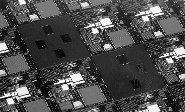
A semiconductor chip
But semiconductors are worth such an effort! Be it in computer sciences, the control of industrial processes, energy technology, information technology, consumer electronics, medical diagnostics, illumination technology or in airplanes, cars, appliances, phones, or watches: semiconductor devices are omnipresent and indispensable. Today, the direct annual market volume of semiconductor devices is about 400 Billion Euro, and the financial impact of semiconductors as a key enabling technology in many other markets is by far larger, still. Also in the future, semiconductors will continue to be a part of our daily life, hopefully with a positive impact. A very visible example in the true sense of the words is the rapid progress in solid state lighting. Here, highly efficient LEDs are replacing more and more the old vacuum tube technology, much in the same way as 50 years ago solid state transistors have replaced vacuum tubes in analogue and digital signal processing. We all witness personally the current progress in computer processors, where Moore’s law is still alive and well. And last but not least semiconductors will help to provide the world population with clean and sustainable energy. At present, solar cells with an accumulated electrical peak power of more than 400 Gigawatt are installed worldwide, the equivalent of about 400 nuclear power plants.

 Walter Schottky Institut