|
Events & News at the Walter Schottky Institute
30 Jun 2025
New News Item
30 Jun 2025
New News Item
14 May 2025
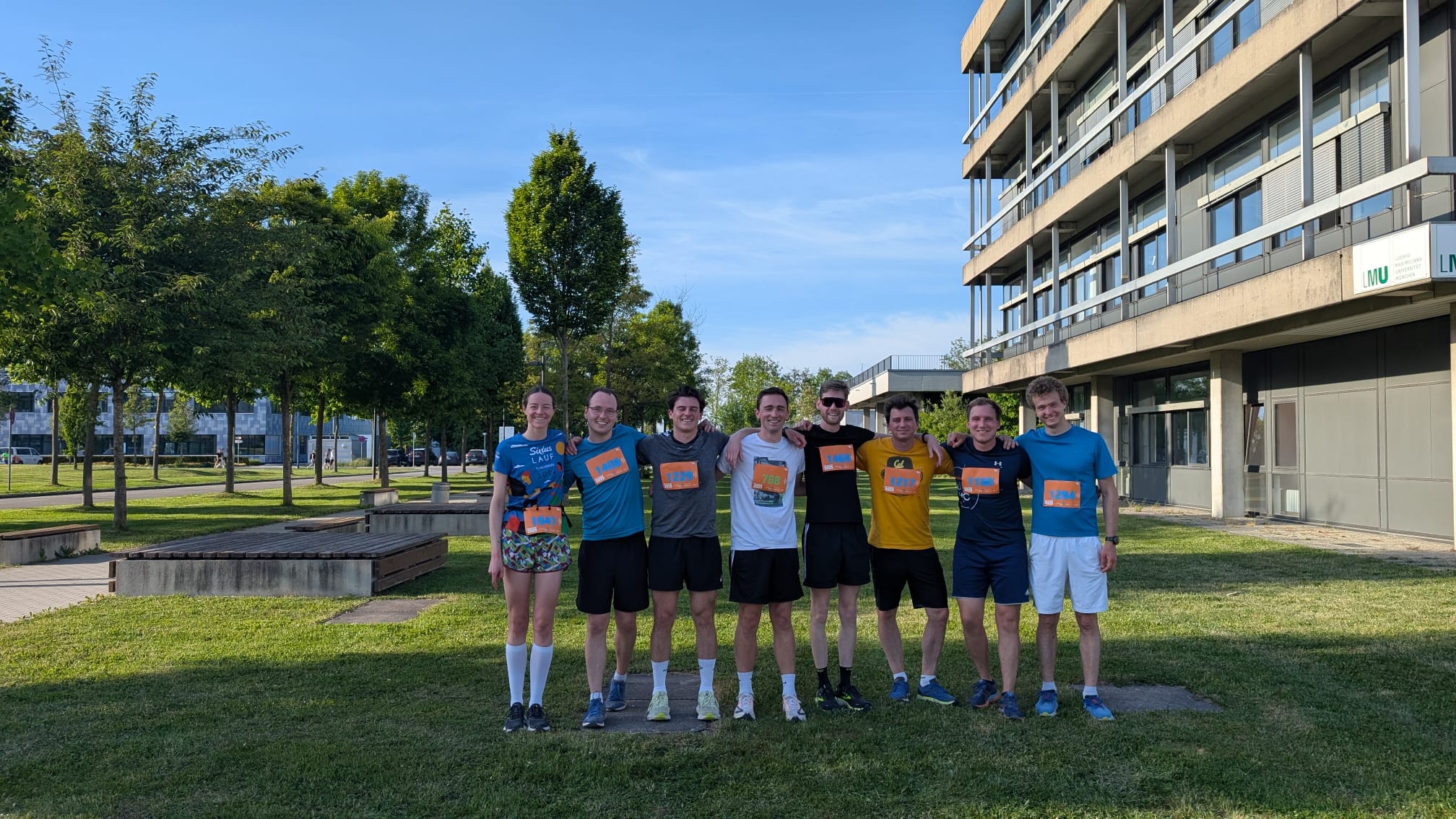
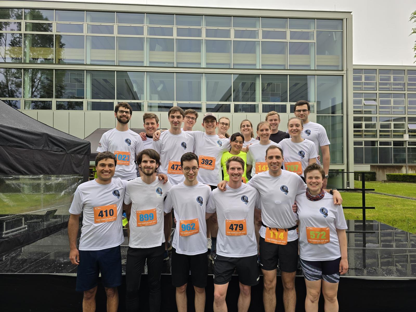
TUM Campus Run 2025
Several teams from the Schottky Institute participated in the Campus Run Lehrstuhl Challenge. Well done! Team E61 finished 29th in 4:22:38 Team Walter Schoki 1 finished 10th in 3:59:55
16 Dec 2024
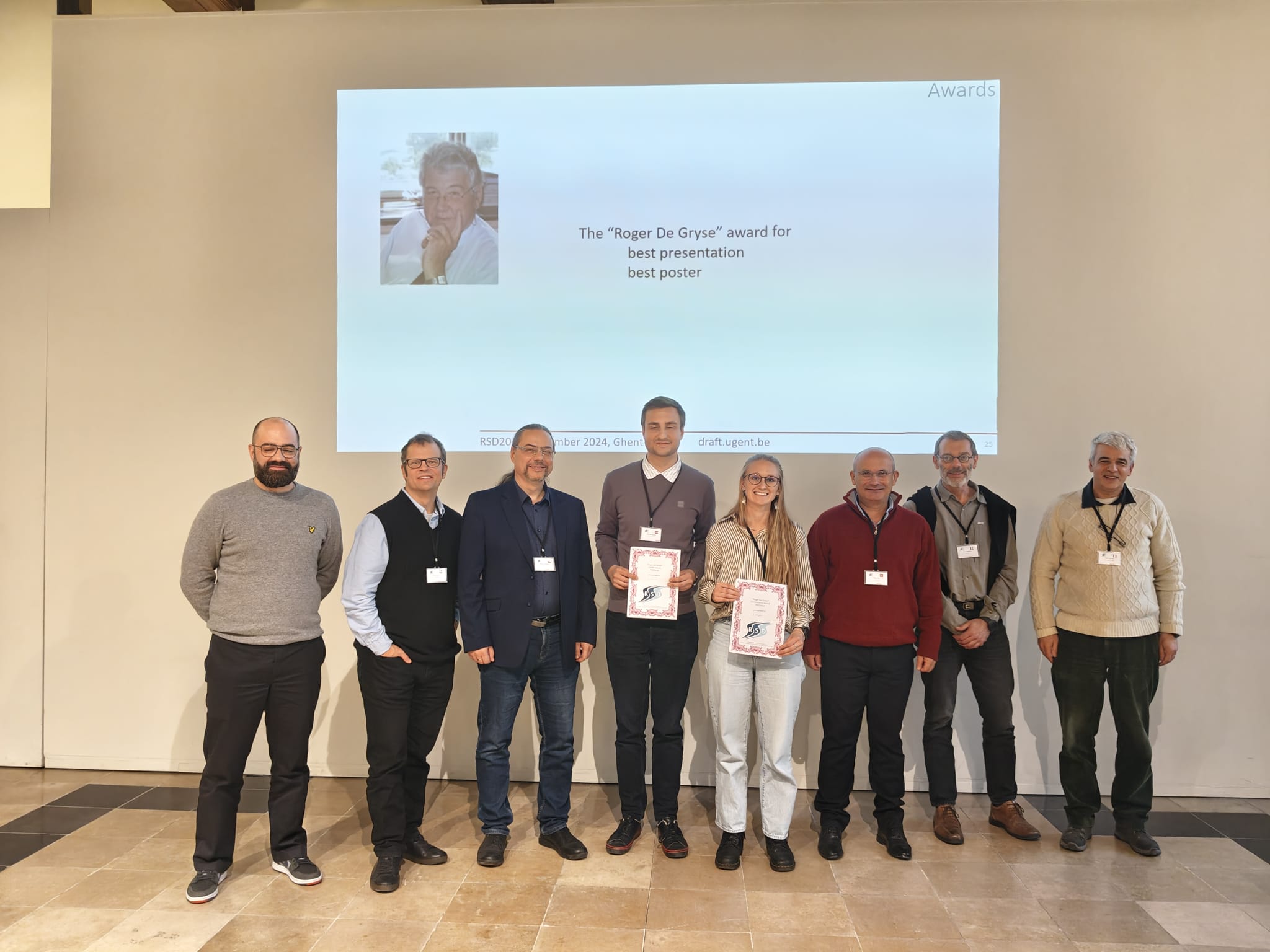
A Hat-Trick for Laura Wagner: Congratulations on Winning another Best Presentation Award
Congratulations to Laura Wagner, who received yet another Best Presentation Award (her third one now, alongside a previous best poster prize too!) at the recent Reactive Sputter Deposition 2024 Conference in Ghent, Belgium. Laura received this well-deserved honour for her work on "Engineering Ti-doped Ta3N5 Photoanodes via Reactive Magnetron Co-Sputtering for Enhanced Solar Fuel Applications." Congratulations Laura and keep up the excellent work!
6 Nov 2024
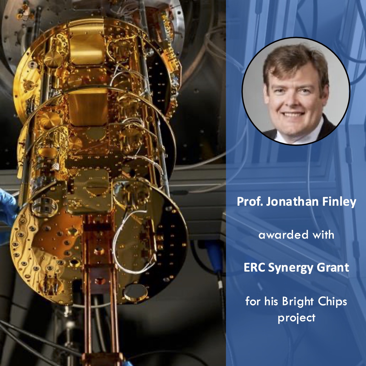
Prof. Jonathan Finley awarded with ERC Synergy Grant!
What an incredible achievement!
Congrats to Jonathan Finley for being awarded the prestigious ERC Synergy Grant! The project “Bright Chips” is a collaboration with Prof. Erik Bakkers (TU Eindhoven) and Prof. Floris Zwanenburg (Uni Twente). Over the next six years, their combined expertise will push the boundaries of light-emitting SiGe-spin qubits. This groundbreaking research promises to unlock new horizons in quantum computing, making chips faster, more scalable, and more resilient for future applications.
The TUM press release can be found: https://www.tum.de/en/news-and-events/all-news/press-releases/details/tum-researchers-secure-two-erc-synergy-grants
28 Sep 2024
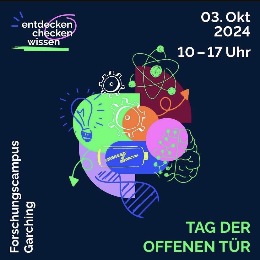
Visit us at the open house at Garching campus on October 3rd
Open house at Garching campus on October 3rd! Meet us at the Walter-Schottky-Insitute and discover our cutting-edge science and technology!
Website: https://forschungscampus-garching.de/
14 May 2024
Fast WSI team at campus run
Our team is not only great in research and teaching - we are also fast! At this year's TUM campus run we participated in the team challenge and placed in the first third of all teams!
28 Apr 2024
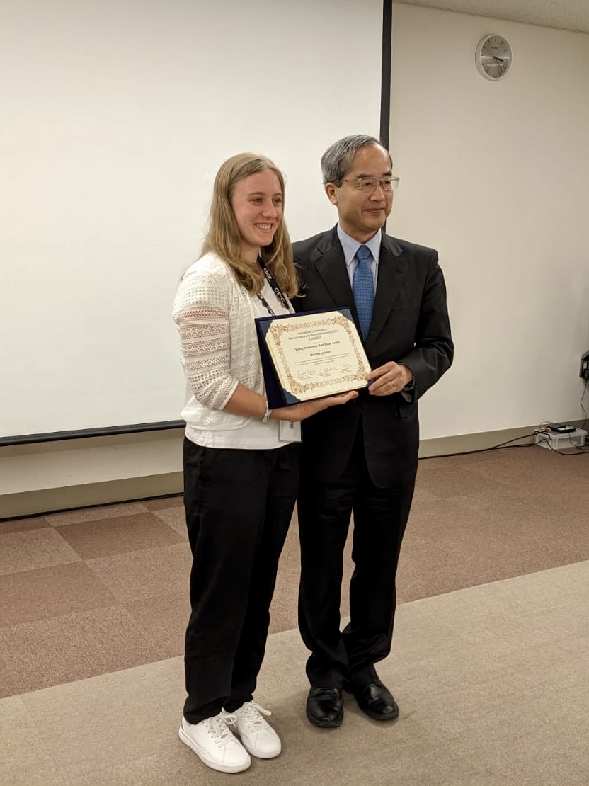
Best oral presentation award for Michelle at the ICNN 2024 conference in Yokohama
Michelle Lienhart gave an excellent talk on „Probing coherent optical response of coupled excitons and spin states in a quantum dot molecule“ at the ICNN conference 2024 in Yokohama and received the best oral presentation award. Congratulations, Michelle!
27 Apr 2024
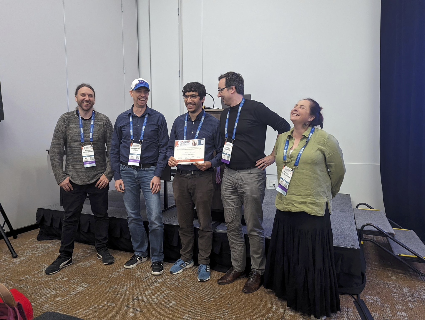
Second best oral presentation award for Amine at MRS spring meeting 2024
Amine Ben Mhenni gave an excellent talk on „Breakdown of the static dielectric screening approximation of Coulomb interactions in atomically-thin semiconductors“ in the QT03 symposium at the 2024 MRS Spring Meeting in Seattle and received the second best oral presentation award.
28 Mar 2024
Poster prizes for Sang Kyu and Michelle at QD 2024
We are happy to anounce that two of the six poster awards at QD2024 go to WSI this year! Congratulations to Sang Kyu Kim and Michelle Lienhart!

14 Feb 2024
BMBF Junior Research Group – CO2UPLED
We are excited to announce the launch of Dr. Verena Streibel’s independent BMBF Junior Research Group CO2UPLED at the Walter Schottky Institute! The efficient transfer of charges across heterogeneous interfaces is critical for sustainable and renewable energy conversion processes. Whether it is generating hydrogen from water splitting or producing carbon-based fuels through CO2 reduction, these reactions demand orchestrated multi-charge transfers across solid|liquid interfaces characterized by generally sluggish reaction kinetics. In photoelectrochemical energy conversion, where sunlight is harnessed to produce fuels, the challenges extend beyond inefficient light absorption, charge recombination, and material instabilities. They also encompass hindered charge transfer due to unfavorable surface chemistries and non-ideal alignments of relevant energy levels. CO2UPLED, short for “Coupling of novel photoelectrode materials to selective catalyst systems for artificial photosynthesis”, is committed to overcoming these hurdles through a knowledge-based approach to interface design. The research program of Dr. Verena Streibel strategically integrates novel thin-film photoelectrode materials based on oxynitrides, transparent catalyst layers, and electrolytes. The methodology employed includes the creation of systematic material libraries, advanced spectroscopy methods under reaction conditions, and theoretical modeling. Ultimately, the project aims to seamlessly incorporate photoelectrode-catalyst couplings into tandem systems for water splitting and CO2 reduction, utilizing sunlight as the exclusive energy source. Contact: Dr. Verena Streibel (WSI, TUM) Funded by the German Ministry of Education and Research (SINATRA: CO2UPLED / 033RC034).
10 Jan 2024
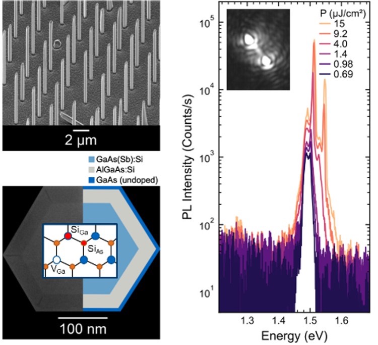
Large tolerance of lasing properties to point defects in GaAs-based nanowire lasers demonstrated
III-V nanowire (NW) lasers are excellent candidates for miniaturized light sources in on-chip optical interconnects, thanks to their unique sub-wavelength geometry and the direct monolithic integration capabilities on silicon (Si) photonic circuits. Over the years of intense research and optimization of resonator design, surface passivation, and minimization of mirror losses, it became clear that the ultimate performance limits will most likely depend on key intrinsic material properties, such as native- and impurity-induced point defects and their impact on non-radiative recombination. To interrogate this, we have now demonstrated the impact of impurity-induced point defects on the lasing properties of low-threshold GaAs(Sb)-AlGaAs core-shell NW-lasers, by exploring Si-dopants and their associated vacancy complexes. As reported in a recent article of Advanced Functional Materials (2023), T. Schreitmüller and co-workers used a combination of methods to identify and correlate type and density of Si-induced point defect complexes with the resulting radiative recombination dynamics and lasing threshold behavior of these NW-lasers. Under very large point defect densities, strong non-radiative Shockley-Read-Hall recombination, reduced carrier lifetime, and lowered IQE (internal quantum efficiencies) was found, which was also reflected by nearly an order of magnitude increased lasing threshold at cryogenic temperatures. However, for intermediate to low point defect densities, the lasing threshold was insensitive to these defects, yielding overall very low threshold < 10 µJ/cm2. Most surprisingly, NW-lasers with high vacancy-defect densities were further found to show superior threshold performance at elevated temperatures with much higher temperature stability and room temperature lasing. These unique characteristics were explained by a suppressed Auger recombination, likely due to the acceptor-type states introduced by the vacancy complexes, which points to a very large tolerance of lasing metrics to impurity defects in these classes of nanolasers.
7 Jan 2024
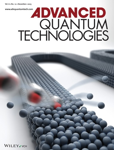
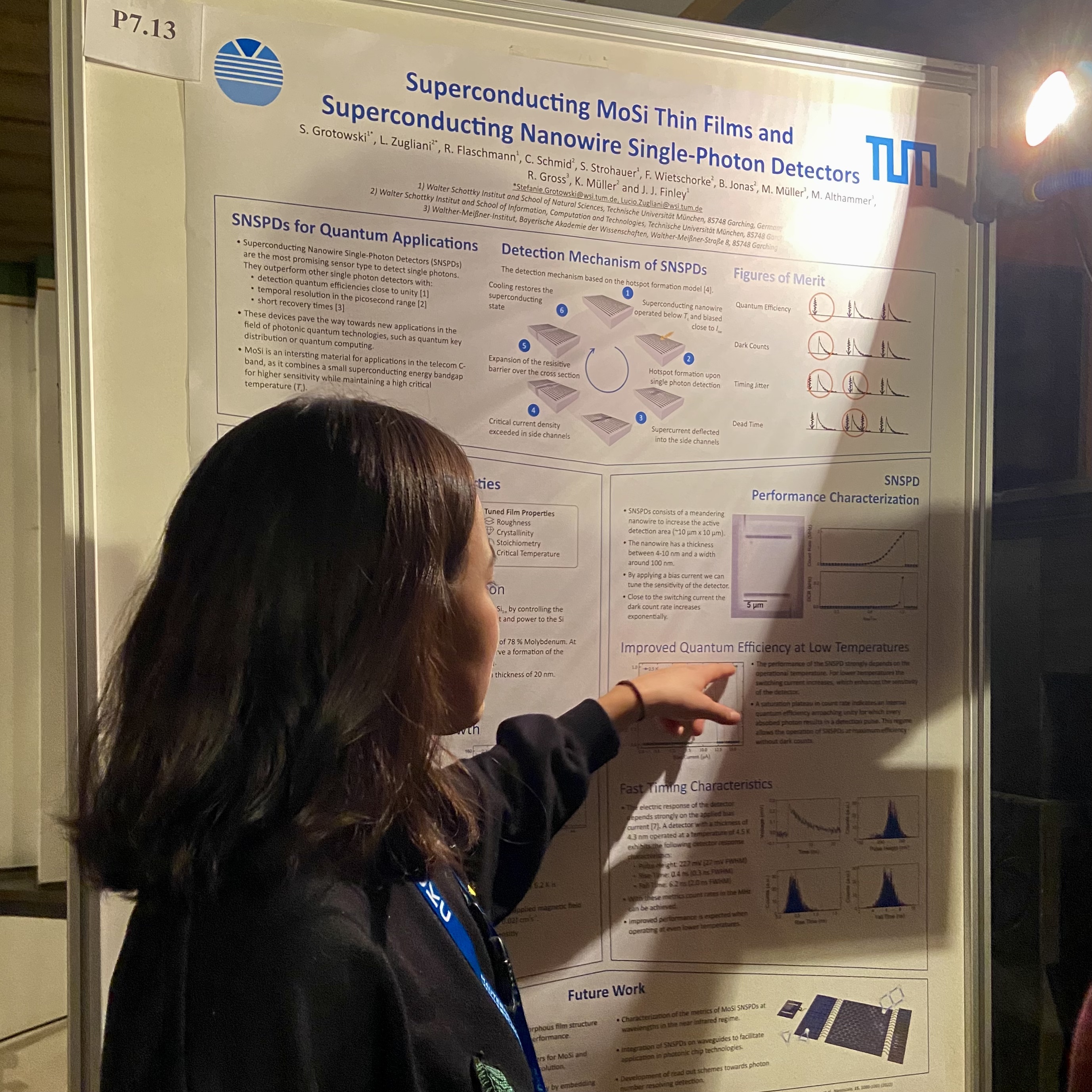
Stefan's paper is on the front cover of Advanced Quantum Technologies
Congratulations to Stefan and his colleagues! Their new paper is published in #Advanced #Quantum #Technologies and even on the cover page! They showed how site-selective helium ion irradiation can be used to tune detection efficiency, switching current, and critical temperature of individual devices on the same chip. For example, the detection efficiency increases from <0.05% to 55.3% after irradiation of a 12nm thick Superconducting Nanowire Single Photon Detector (SNSPD). The cover illustrates an SNSPD that is bombarded with a beam of helium ions, which modify the device by introducing defects into the nanowire and sputtering off atoms of the superconducting material.
Cover image by Christoph Hohmann (MCQST).
Check out the paper here: https://onlinelibrary.wiley.com/doi/10.1002/qute.202370121
20 Dec 2023
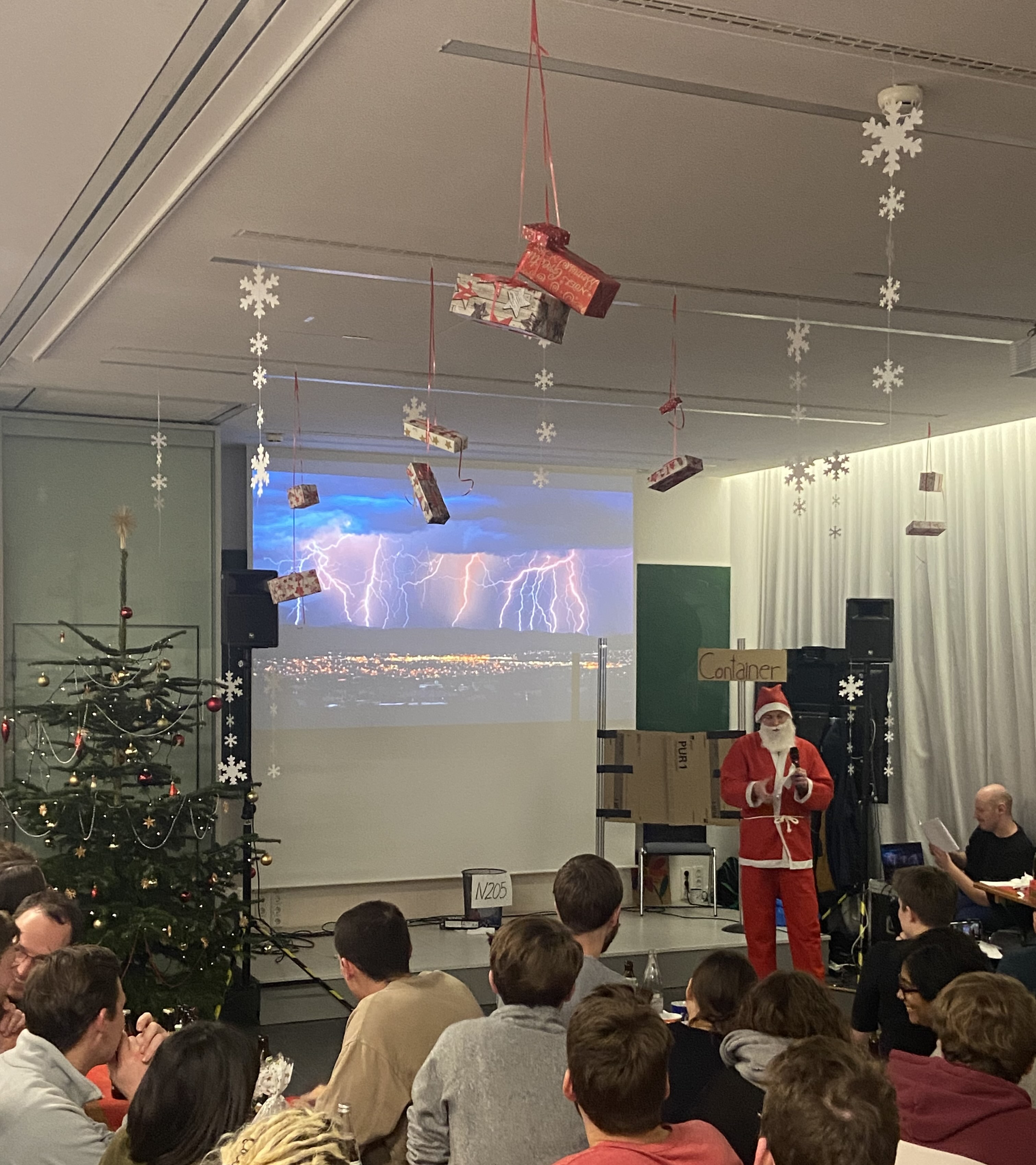
WSI Christmas party
Last week, we had a wonderful Christmas party at WSI! Good food, amazing performances, and lots of fun. Even Santa Claus came to visit us. Merry Christmas to everyone!
1 Nov 2023
ERC starting grant 2DTopS
One of the pillars of today’s nanotechnology is the ability to precisely control the spatial symmetries and spatial extents of quantum states confined into nanostructures, either by top-down or bottom-up approaches. An intriguing case are superlattice structures, where a nanoscale periodic potential is superimposed onto the periodic atomic arrangement of a solid-state material. These superlattices give rise to artificial condensed matter phases with emergent quantum electronic properties fully controlled by the shape, magnitude and symmetry of the external potential. In the ERC starting grant project "Top-Down Superlattice Engineering of 2D Solid-State Quantum Matter ", 2DTopS, a research team led by Dr. Christoph Kastl investigates now the emergent quantum states in such nanofabricated superlattice structures. To achieve the required fabrication precision of few nanometers, the team makes use of state-of-the-art clean room and nanofabrication capabilities at the Center for Nanotechnology and Nanomaterials, including a helium ion microscope and a newly installed 100 keV electron beam lithography system. The project focuses on two-dimensional materials with strong spin-orbit coupling and non-trivial band topologies to establish the potential as functional spin-electronic and optoelectronic devices in semiconductor and quantum technologies.
contact: Dr. Christoph Kastl (WSI, TUM)
Funded by the European Union (ERC, 2DTopS, 101076915). Views and opinions expressed are however those of the author(s) only and do not necessarily reflect those of the European Union or the European Research Council Executive Agency. Neither the European Union nor the granting authority can be held responsible for them.
1 Oct 2023
ERC starting grant DynNano
A promising approach to directly convert sunlight into storable fuels is photoelectrochemical energy conversion. Economically viable and scalable photosystems are often based on semiconducting thin films. These photoelectrodes exhibit locally varying material properties, from the nanoscale to the microscale. To date, typical macroscale characterization techniques average the performance and fundamental properties over the whole photoelectrode and conceal important nanoscale insights. The DynNano research program of Dr. Johanna Eichhorn will leverage a complementary suite of advanced nanoscale microscopy and spectroscopy techniques to reveal the local processes of semiconductor photoelectrodes under realistic operation conditions. The gained comprehensive portrait of the elementary steps associated with light-to-chemical energy will provide the knowledge basis for rational development of efficient, stable, and scalable solar fuel devices. contact: Dr. Johanna Eichhorn (TUM)
TUM press release
Project in Cordis Funded by the European Union (ERC, DynNano, 101076858). Views and opinions expressed are however those of the author(s) only and do not necessarily reflect those of the European Union or the European Research Council Executive Agency. Neither the European Union nor the granting authority can be held responsible for them.
19 Sep 2023
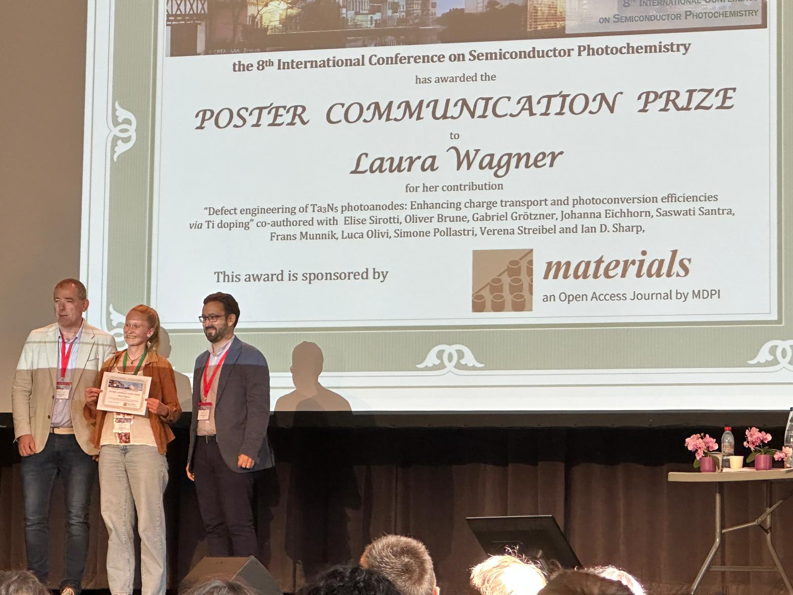
Congratulations to Laura Wagner, Awarded Prize at SP8 Conference
Congratulations to Laura Wagner, who received the Poster Communication Prize for her work entitled "Defect Engineering of Ta3N5 Photoanodes: Enhancing Charge Transport and Photoconversion Efficiencies via Ti Doping" at the 8th International Conference on Semiconductor Photochemistry in Strasbourg, France. Great work and congratulations on the well-deserved honor, Laura!
4 Jul 2023
Pedro Soubelet awarded with Walter-Benjamin fellowship
We are excited to share that our Postdoc Pedro Soubelet has been awarded a Walter-Benjamin fellowship! He will explore many-body interactions in one-dimensional dipolar exciton gases defined in atomically thin semiconductors.
29 Jun 2023
GESUCHT: Techniker/in (vollzeit, unbefristet)
Der Lehrstuhl für "Halbleiter-Nanostrukturen und Quantensysteme" (Prof. Dr. J. J. Finley) am TUM-Zentralinstitut Walter Schottky Institut sucht zum nächstmöglichen Zeitpunkt eine/n Techniker/in (m/w/d) auf Vollzeitbasis. Ihr Aufgabengebiet: · Anwendung modernster Strukturierungs- und Nanotechnologien-Verfahren (Elektronenstrahl- und Ionenstrahl-Lithographie) zusammen mit Wissenschaftler/innen, Studenten und Studentinnen. · Betreuung und Wartung von Halbleiter-Prozessanlagen. · Selbständige Prozessierung von opto-elektronischen Halbleiter-Bauteilen · Integration von wissenschaftlich-technischen Geräten und deren Steuerungen · Mitarbeit bei der praktischen Durchführung von wissenschaftlichen Experimenten Unser Angebot: · Selbständiges Arbeiten mit verantwortungsvollen Aufgaben in einem sehr internationalen, dynamischen wissenschaftlichen Umfeld. · Kollegiale Atmosphäre mit flachen Hierarchien sowie viel Handlungs- und Mitgestaltungsspielraum. · Attraktives Gehalt nach TV-L (Entgeltgruppe und Stufe je nach persönlicher Eignung und Berufserfahrung – zzgl. Jahressonderzahlung und Option einer Leistungsprämie) in einem unbefristeten Beschäftigungsverhältnis · Einarbeitung durch eine erfahrene Fachkraft. · Interne Fortbildungen zu Ausbau von Fachkompetenzen und Soft-Skills. · Geregelte Arbeitszeiten, bis zu 30 Urlaubstage. · Lebendiges und wissenschaftliches Umfeld als Mitglied einer internationalen Forschungsgruppe. Ansprechpartner: Bei Fragen stehen wir gerne telefonisch (Tel.: 089/289-12770) oder per E-Mail (jj.finley@tum.de) zur Verfügung. Bitte senden Sie uns Ihre Bewerbungsunterlagen per E-Mail in einer pdf-Datei an jj.finley@tum.de
29 Jun 2023
GESUCHT: Teamassistenz (vollzeit, unbefristet)
Der Lehrstuhl für "Halbleiter-Nanostrukturen und Quantensysteme" (Prof. Dr. J. J. Finley) am TUM-Zentralinstitut Walter Schottky Institut sucht zum nächstmöglichen Zeitpunkt eine/n Teamassistenz (m/w/d) auf Vollzeitbasis. Ihr Aufgabengebiet: · Organisation und Administration von Studienangelegenheiten · Administrative Betreuung von Forschungsprojekten, inkl. Buchung in SAP · Betreuung des Publikumsverkehrs Ihr Profil: · Eine kaufmännische oder verwaltungstechnische Ausbildung mit einschlägiger Berufserfahrung oder Erfahrung in einer vergleichbaren Position · Ein freundlicher, professioneller Umgang als Schnittstelle zwischen Studierenden, Lehrenden, Gästen, externen Projekt- und Geschäftspartnern · Organisationstalent, Zahlenverständnis und ein eigenständiger und lösungsorientierter Arbeitsstil · Teamfähigkeit · Kenntnisse im Umgang mit aktuellen Microsoft Office Produkten (Excel, Word) · Sehr gute Kenntnisse der deutschen und Kenntnisse der englischen Sprache Unser Angebot: · Einen modernen Arbeitsplatz und eine interessante, abwechslungsreiche Beschäftigung in einem sehr internationalen Umfeld · Bezahlung nach dem TV-Lin einem unbefristeten Beschäftigungsverhältnis · Flexible Arbeitszeiten Ansprechpartner: Bei Fragen stehen wir gerne telefonisch (Tel.: 089/289-12770) oder per E-Mail (jj.finley@tum.de) zur Verfügung. Bitte senden Sie uns Ihre Bewerbungsunterlagen per E-Mail in einer pdf-Datei an jj.finley@tum.de
24 May 2023
Alain Dijkstra awarded with Marie Skłodowska-Curie fellowship
We are thrilled to share that our Postdoc Alain Dijkstra has been awarded a Marie Skłodowska-Curie fellowship. Since the first of April he is working as a fellow in the group of Jonathan Finley at our institute. During his time at the WSI, he will be investigating the interactions of interlayer-excitons in 2D materials (transition metal dichalcogenides TMDs in particular). The huge exciton binding energies that excitons experience in 2D-materials make this the perfect platform to study these quasi-particles, as this makes them extraordinarily stable. With the understanding of their interactions, wehewill start manipulating and controlling them. Because excitons are quantum particles, they can mimic other quantum systems. By trying to take full control of them, the initial steps are taken towards a versatile platform for quantum simulation.
24 May 2023
New News Item
23 May 2023
New News Item
28 Mar 2023
Congratulations to Eugenio Zallo's newest paper published in Springer Nature!
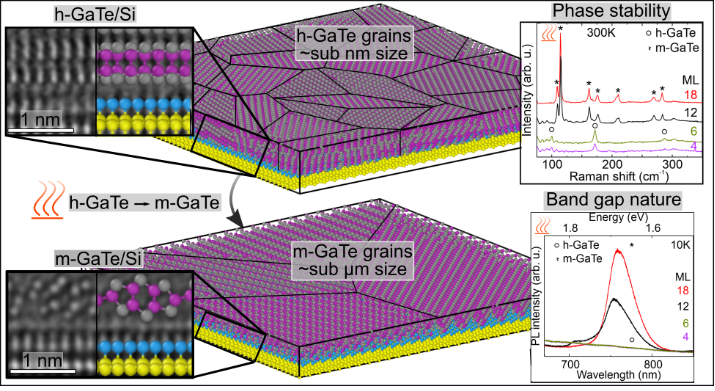
In our recent publication in npj 2D Materials and Applications (https://rdcu.be/c8u8o) we demonstrate the formation of atomically sharp interface and single crystal m-GaTe on the silicon substrate by using a two-step technique based on the phase transformation of h-GaTe. The control of both unstable phases and 2D anisotropic semiconductors on standard crystalline wafers may be a key ingredient for next-generation quantum and optoelectronic devices and novel thin layer-based multifunctional systems. The work has been carried out in collaboration with CNR Rome, INFN, MIET, and the Universities of Rome Tor Vergata and Milano Bicocca.
3 Mar 2023
Congratulations to Dr. Verena Streibel, Appointed to the Junges Kolleg der BAdW!
Congratulations to Dr. Verena Streibel on her selection to the prestigious Junior Research Council of the Bavarian Academy of Sciences (Das Junge Kolleg der Bayerischen Akademie der Wissenschaften)! Verena's research within the Council is devoted to developing renewable energy conversion systems, with a particular focus on understanding complex charge transfer processes at transition metal oxynitride interfaces during photoelectrochemical water splitting. The Junior Research Council was created in 2010 to support excellent young scientists at the post-doctoral research stage. This well-deserved honor provides an initial term of three years with opportunity for close exchange with leading Bavarian scientists across multiple disciplines. More information can be found here.
27 Feb 2023
International summer graduate school on nanotechnology and nanomaterials
The intention of this summer school is to
discuss recent developments in the photo-physics of nanoscale materials
with a specific focus on two-dimensional layered materials and their
opto/spin-electronic properties. Date: 01.07.-08.07.23 Location: Fetovaia For more information, contact Prof. Holleitner.
21 Feb 2023
Mauterndorf Winterschool 2023
After 3 years, we are excited to return to the Mauterndorf Winterschool on New Developments in Solid State Physics. Lots of great talks, discussions, and poster presentations! We are also very proud our PhD students Philipp Moser and Stefanie Grotowski won the famous ski race in Mauterndorf!
25 Nov 2022
Quantum Sensing workshop brings together scientist from Garching
Today and next Friday (02.12.22), we have organized a workshop on Quantum Sensing to get an overview of the activities in Garching in this direction.
It is organized in the framework of the Munich Center for Quantum Science and Technology (MCQST), the Munich Quantum Valley (MQV) and the Zentrum für Quantum Engineering of TU München (ZQE).
Looking forward to great talks and many fruitful discussions!
18 Nov 2022
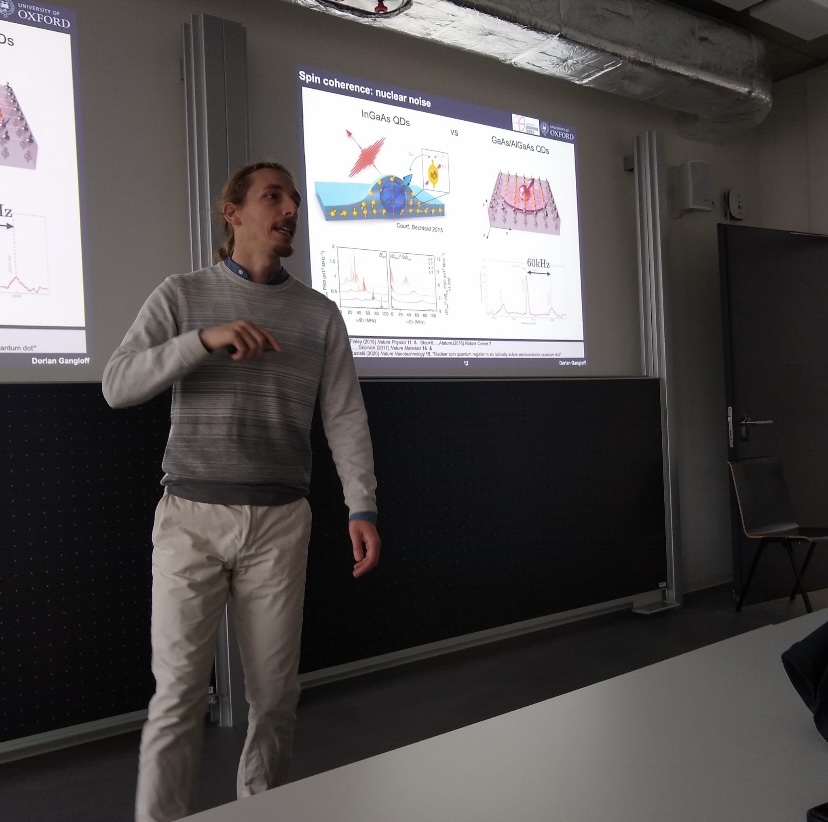
Dorian Gangloff from Oxford visiting WSI
It was great having a brilliant scientist like Dorian Gangloff from University of Oxford at WSI. Thanks for the great talk on quantum control of spin-photon interfaces!
17 Nov 2022
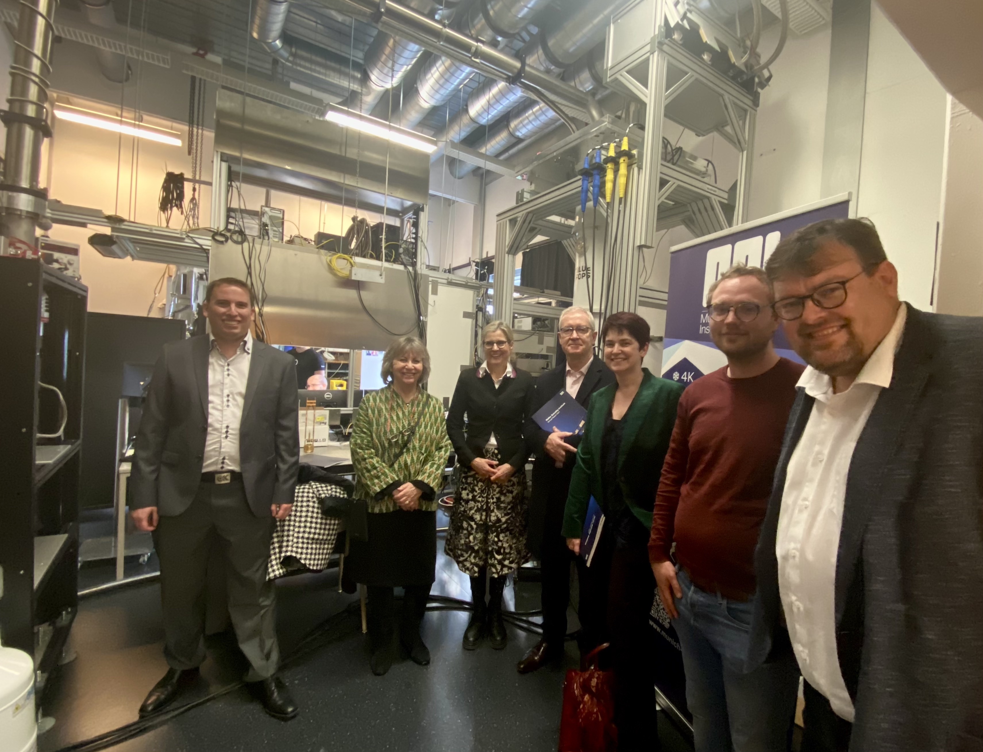
High visit: TUM and Imperial College President at WSI
On Thursday, November 18th, 2022, the President of Imperial College London (Professor Hugh Brady) and Senior Vice President of the Technical University of Munich (Professor Juliane Winkelmann) visited the Walter Schottky Institut.
It was an honor having such high visit at WSI and guiding you through our labs!
Background of their visit: Imperial College London (Imperial) and the Technical University of Munich (TUM) want to work together on a new economy without pollution. The Imperial - TUM Zero Pollution Network will bring together scientists, industry, governments and other partners. The goal is to curb environmental pollution at its source. For example, the life cycle of technologies and products will be taken into account: from the procurement of raw materials to their further processing in industry and their use in society to their disposal and reuse.
Read more on: https://www.tum.de/en/news-and-events/all-news/press-releases/details/eine-wirtschaft-ohne-umweltverschmutzungen On the picture (from left to right): Prof. Kai Müller, Imperial Vice President Maggie Dallman, TUM Senior Vice President Prof. Juliane Winkelmann, Imperial President Prof. Hugh Brady, Imperial Vice-Provost Prof. Mary Ryan, Rasmus Flaschmann, Prof. Jonathan Finley.
10 Nov 2022
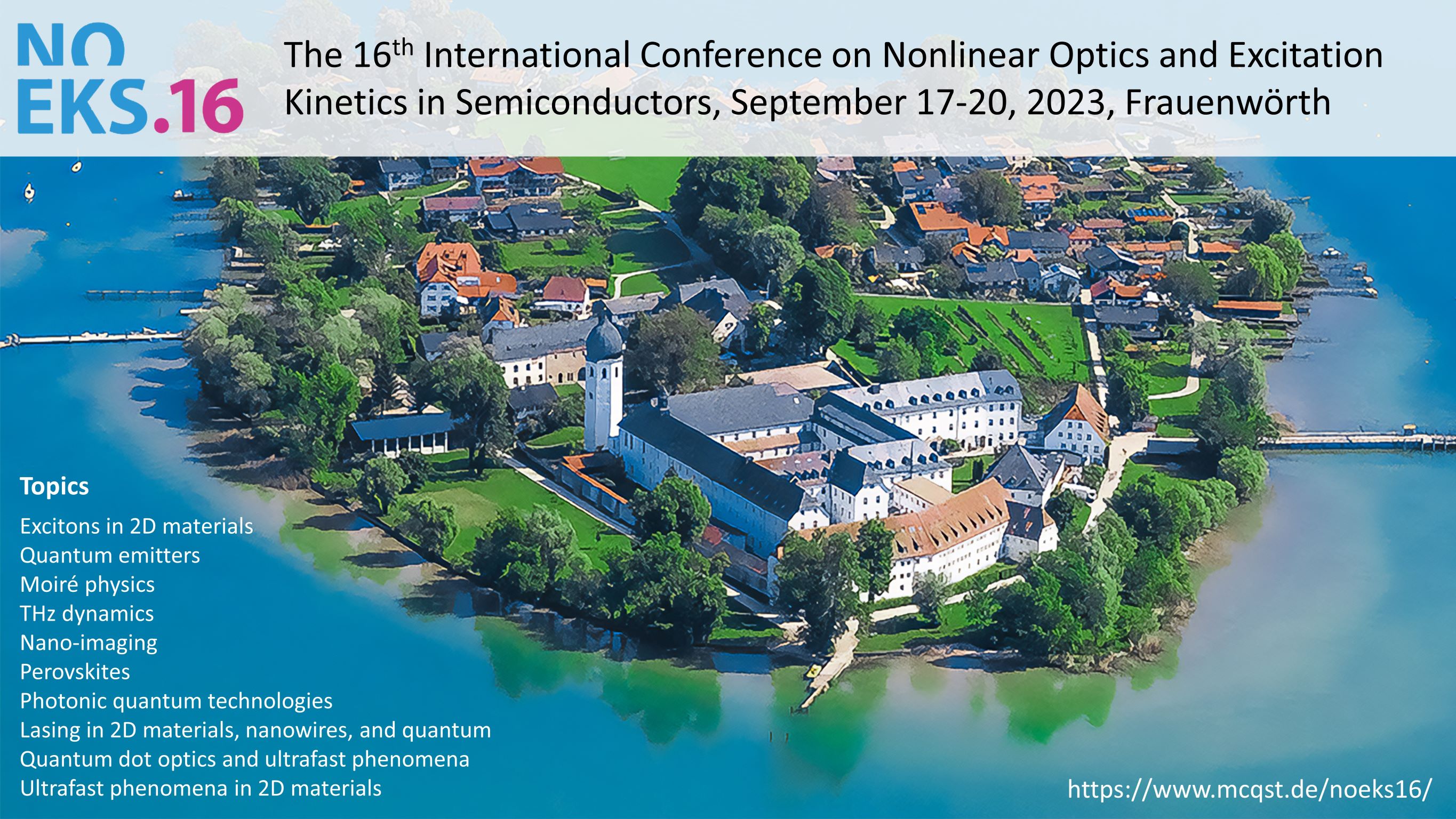
WSI hosts NOEKS16 in 2023
The WSI proudly organizes the 16th version of "The International Conference on Nonlinear Optics and Excitation Kinetics in Semiconductors" (NOEKS16) at the venue www.frauenwoerth.de from September 17 to 20, 2023. For more information, please check: www.mcqst.de/noeks16/
The local conference committee
Christoph Kastl & Alexander Holleitner
1 Oct 2022
New European research project ONCHIPS: Interplay of electronics and photonics for next generation quantum devices
New European research project ONCHIPS: Interplay of electronics and photonics for next generation quantum devices
For building quantum computers, applying both, electronics and photonics – technology that works with light – on one and the same chip, is promising. By utilizing silicon the platform we know well from today’s electronic devices, quantum devices could be protected from influences from the outside world. Another advantage is that silicon-based devices can be scaled up to larger systems. Unfortunately, light and silicon are not best friends. Adding germanium to the silicon, however, forms a fully new crystal structure. In that case, electronic and photonic quantum bits can indeed be combined in one device. In the scope of this new European research project ONCHIPS, the group of Professor Jonathan Finley at the Walter Schottky Institute (Technische Universität München) will work on applying silicon for quantum devices. Making predictions about the best manufacturing technology for quantum computers is not easy: all approaches have their pro’s and con’s. Some of the quantum bits (qubits) are quite large, need extreme cooling, and are very sensitive to their surroundings: there’s only a short time in which you can benefit from their specific quantum properties. Others are more robust and less sensitive to disturbances but can’t easily be upscaled to thousands or even millions of qubits. What you, in fact, would like to do, is benefit from the industrial scale and highly standardized processes used for ‘regular’ semiconductor chips (CMOS). In the combination of silicon and germanium, recently discovered, may combine many of the advantages on one chip. This material, having a particular hexagonal crystal structure, was awarded breakthrough of 2020 by Physics World. The inventors of the material, of the Technical University of Eindhoven (Netherlands), are a member of the new ONCHIPS consortium. Energy levelsThe hexagonal structure of silicon-germanium has a major advantage: it enables silicon to send and absorb light. In this way, photons can be coupled to electrons that owe their quantum qualities to their ‘spin’: the direction in which they toll around their own axis. This opens whole new possibilities, for example in combining the superior quantum transport properties of photons and the local quantum calculation power of electrons. And all this on the same CMOS electronics chip. One of the problems still to be solved is that creating the hexagonal structure must be done in an easier way than is feasible right now. What silicon on its own can’t do, and the combination of silicon and germanium can, is associated with the ‘direct band gap’ that is created in this way. An electron can directly cross a barrier between two energy levels and send out a photon by doing so. Silicon itself does not have this direct band gap: the energy levels are not directly above each other, so silicon itself is not a good light source. New materials, new building blocksThe direct band gap approach of silicon may lead to exciting new perspectives in quantum computing, although it is still a challenging task. Professor Floris Zwanenburg, from the University of Twente and project leader of the ONCHIPS consortium, says. “Each of our ideas have never been realized in this way. The ambition is understanding more about the best conditions for crystal growth. Furthermore, we have to create the first spin qubits and shape interfaces of these spin qubits and photons. Thorough understanding of the germanium silicon crystal structure is key.” And all that with the future integration of electronics and photonics in mind, on one and the same silicon platform.
Partners in this new European program, next to the Walter Schottky Institute of the TU München (Germany) and University of Twente (Netherlands), are TU Eindhoven (Netherlands), Centre National de la Recherche Scientifique (CNRS, France), Dutch company Single Quantum, Universität Konstanz (Germany) and Budapest University of Technology and Economics (Hungary).
9 Jun 2022
Best Student Presentation Award at MRS Spring 2022 for Laura Wagner
Congratulations to Laura Wagner, who received the Best Student Presentation Award at the MRS Spring 2022 symposium on "Emerging Inorganic Semiconductors for Solar Energy and Fuels" for her talk on "ZrTaN3 - A New Visible Light Absorbing Ternary Nitride Semiconductor Photoelectrode." Great work, Laura!
7 Oct 2021
BMBF project on Quantum LifeLong Learning (QL³)
Quantum technologies comprise rapidly growing scientific fields with great potential for applications in industry. The current challenge for Germany and Europe is to educate a sufficiently large number of students in quantum technologies and to transfer knowledge as well as technological expertise from the research laboratories to the industrial sector. A key role is played by the specialists and executives of the high-tech industry, who have to recognize and implement the specific potential of quantum technologies for the respective company.
The BMBF funded project Quantum LifeLong Learning (QL³) developes a targeted education and training program of the Munich universities in the field of quantum technologies according to a university certificate and ECTS system with the target group of specialists and executives in industry. In close cooperation with an industrial advisory board and university didactics experts, world-renowned researchers create educational concepts and programs to jointly advance this new topic in adult education at the interface between cutting-edge research and product development.
Innovation and perspectives In cooperation with an industrial advisory board, the modules will be developed according to industrial needs and thus market value. In a mid-term perspective, the programm will run at the TUM Institute for LifeLong Learning (TUM IL³).
Funded by the BMBF under contract 13N15996 contact: Prof. A.W. Holleitner (TUM) and Prof. Jan von Delft (LMU) https://www.quantentechnologien.de/forschung/foerderung/quantentechnologien-foerderung-von-forschungsarbeiten/transqnode-1.html Figure: Quantum technologies rely on high-end measurement systems, such as ultra-cold crystats, C. Hohmann, MCQST.
7 Jun 2021
Atom swapping paves way for bright, flexible next generation LEDs
An
international group of researchers has developed a new technique that could be
used to make more efficient low-cost light-emitting materials which are
flexible and can be printed using ink-jet techniques.
The
researchers, led by the University of Cambridge and the Technical University of
Munich, found that by swapping one out of every one thousand atoms of one
material for another, they were able to triple the luminescence of a new
material class of light emitters known as halide perovskites.
This ‘atom
swapping’, or doping, causes the charge carriers to get stuck in a specific
part of the material’s crystal structure, where they recombine and emit light. The
results,
reported in the Journal of the American Chemical Society, could be useful
for low-cost printable and flexible LED lighting, displays for smartphones or
cheap lasers.
Many everyday applications
now use light-emitting devices (LEDs), such as domestic and commercial lighting,
TV screens, smartphones and laptops. The main advantage of LEDs is they consume
far less energy than older technologies.
Ultimately,
also the entirety of our worldwide communication via the internet is driven by
optical signals from very bright light sources that within optical fibres carry
information at the speed of light across the globe.
The team studied
a new class of semiconductors called halide perovskites in the form of
nanocrystals which measure only about a ten-thousandth of the thickness of a
human hair. These ‘quantum dots’ are highly luminescent materials: the first
high-brilliance QLED TVs incorporating quantum dots recently came onto the
market.
The Cambridge
researchers, working with Daniel Congreve’s group at Harvard, who are experts
in the fabrication of quantum dots, have now greatly improved the light
emission from these nanocrystals. They substituted one out of every one
thousand atoms with another – swapping lead for manganese ions – and found the
luminescence of the quantum dots tripled.
A detailed
investigation using laser spectroscopy revealed the origin of this observation.
“We found that the charges collect together in the regions of the crystals that
we doped,” said Sascha Feldmann from Cambridge’s Cavendish Laboratory, the
study’s first author. “Once localised, those energetic charges can meet each
other and recombine to emit light in a very efficient manner.”
“We hope this
fascinating discovery: that even smallest changes to the chemical composition
can greatly enhance the material properties, will pave the way to cheap and
ultrabright LED displays and lasers in the near future,” said senior author
Felix Deschler, who is jointly affiliated at the Cavendish and the Walter
Schottky Institute at the Technical University of Munich. What are the next steps?
In the future
the researchers hope to identify even more efficient dopants which will help
making these advanced light technologies accessible to every part of the world.
Reference:
Sascha
Feldmann et al. ‘Charge carrier
localization in doped perovskite nanocrystals enhances radiative recombination.’,
Journal of the American Chemical Society (2021). DOI: 10.1021/jacs.1c01567

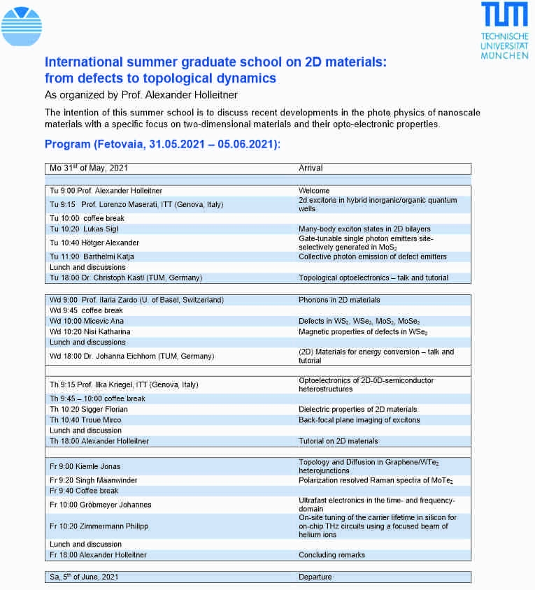
31 May 2021
International summer graduate school
The intention of this summer school is to discuss recent developments in the photo-physics of nanoscale materials with a specific focus on two-dimensional materials and their opto-electronic properties. Date: 31.05.-05.06. Location: Fetovaia For more information, contact Prof. Holleitner.
5 Oct 2020
WSI - MCQST Diversity Event
On 16 October at 3 p.m - WSI will be hosting an online Diversity Coffee at WSI in close collaboration with the DFG cluster of Excellence MCQST. Barbara Tautz will give a short introduction to MCQST's support programs and she is looking forward to getting to know you and exchanging ideas on topics such as gender equality, mental health, and family and career at WSI afterward.
Please register till 15 October via https://www.mcqst.de/news-and-events/events/diversity-coffee-at-wsi.html.
3 Jun 2020
Congratulations to Dr. Johanna Eichhorn!
Congratulations to Dr. Johanna Eichhorn on her selection to the prestigious Junior Research Council of the Bavarian Academy of Sciences (Das Junge Kolleg der Bayerischen Akademie der Wissenschaften)! The Junior Research Council was created in 2010 to support excellent young scientists at the post-doctoral research stage. This well deserved honor provides an initial term of three years with opportunity for close exchange with leading Bavarian scientists across multiple disciplines. More information can be found here.
16 Jan 2020
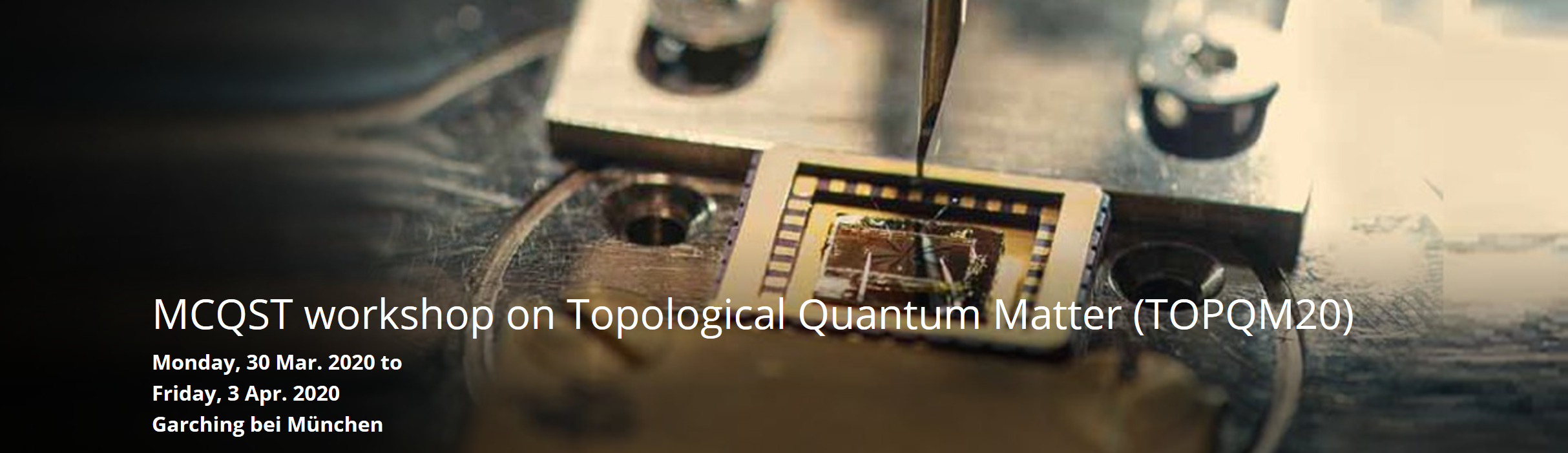
MCQST Conference on Topological Quantum Matter
MCQST members Alexander Holleitner, Monika Aidelsburger, Christoph Kastl and Frank Pollmann are organising the 1st MCQST Conference on Topological Quantum Matter, March 30 - 03 April 2020.
The main goal of the workshop is to bring together
leading scientists working on topological phases in condensed matter
systems, with an emphasis on phenomena which arise due to the interplay
of symmetry and topology. The purpose is twofold: on the one hand, we
want to bring together experts to report on their progress and to
discuss future directions, and on the other hand provide an opportunity
for new-coming PhD students and young postdocs to learn about recent
developments in the field. Registration is now open and free of charge. Selected contributions will be accepted as contributed talks. The conference will take place at the Institut of Advanced Studies in Garching. Submit your abstract and register here.
The focus of the workshop includes the following topics:
Higher order topological phases Crystalline Topological Insulators Realization of topologically phases in optical lattices and new quantum materials Novel phases in twisted multilayer materials Symmetry protected / enriched topological phases Artificial gauge fields Topological quantum computing
Invited speakers
- Nigel Cooper | Cambridge University
- Hannah Price | University of Birmingham
- Ian Spielman | NIST
- Christof Weitenberg | Hamburg University
- Erez Berg | Weizmann Institute
- Ignacio Cirac | Max Planck Institute of Quantum Optics
- Michael Knap | TU Munich
- Moty Heiblum | Weizmann Institute
- Christian Pfleiderer | TU Munich
- Radu Coldea | University of Oxford
- Lucile Savary | ENS Lyon
- Matthias Punk | LMU Munich
- Norbert Schuch | TU Munich
- Titus Neupert | University of Zurich
- Fabian Grusdt | LMU Munich
- Yizhi You (tbc) | Princeton
- Felix von Oppen | FU Berlin
- Thomas Schmidt | University of Luxembourg
- Maia Vergniory | DIPC San Sebastian
- Claudia Felser | CPFS Dresden
- Xie Chen | Caltech
- Mitali Banerjee | Weizmann Institute
- Robert König | TU Munich
- Michael Zaletel (tbc) | UC Berkeley
- Ingrid Mertig | University Halle
- James Analytis | UC Berkeley
- Roni Ilan | Tel Aviv University
- Sergej Moroz | TU Munich
2 Jan 2020
New EU-FET Open Project - QLUSTER !
The new EU FET-Open project QLUSTER focuses on developing entirely new approaches to produce many entangled photons with exponentially improved scaling efficiencies. Hereby, a European consortium will make use of the spin of charge carrier(s) trapped in semiconductor artificial atoms and molecules to efficiently produce one- and two-dimensional streams of entangled photons. The project is coordinated by Wolfgang Löffler (U. Leiden) and involves the groups of Dirk Bouwmeester (Leiden), Pascale Senellart (CNRS), WSI professors Jonathan Finley (TUM, PH) and Kai Müller (TUM, ECE), Claire Le Gall & Mete Atatüre (U. Cambridge), Richard Warburton (Basel), Sophia Economou (FORTH, Heraklion, Crete) and Hagai Eisenberg (Hebrew University, Jerusalem). All of us in WSI are excited to be embarking on this project with such a great team !
2 Jan 2020
New German-Israeli DFG Collaborative Project
We are excited to be starting a new TUM-Technion collaborative project funded by the DFG for the next five years. The project entitled Bright Sources of Quantum Light for Efficient Entanglement Distribution is led by Netanel Lindner (Technion) and Jonathan Finley (TUM, PH) and involves the groups of Kai Müller (TUM, ECE), Sven Höfling (U. Würzburg) and David Gershoni (Technion). The project focuses on the development and testing of semiconductor devices capable of generating so-called photonic cluster states for "measurement based" quantum technologies. We are very much looking forward to start working in this exciting project with our collaborators and friends at Technion.
2 Jan 2020
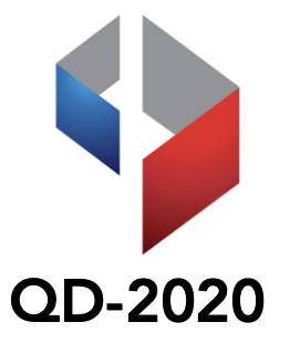
QD2020 International Conference
WSI Professors Jonathan Finley and Kai Müller are organising the 11th International Conference on Quantum Dots (QD-2020) 7-11 December 2020 (Shifted from May due to CoViD-19 outbreak) QD2020 is the leading conference bringing together leading researchers working on the fundamental physics, material, synthesis and applications of Quantum Dots in both experiment and theory. Scientific topics include : - Fundamentals: ab-initio and effective theories, spin and magnetic phenomena, quantum optics, quantum coherence, as well as novel analytical and spectroscopic methods…
- Materials: epitaxial & chemically synthesized dots, nanoplatelets, atomically thin 2D materials, layered perovskites and hybrid organic / inorganic QD nanosystems
- Applications: quantum information technologies, energy harvesting, light-emission, sensors, detectors and biosciences….
We are looking forward to hosting this conference - it will be a lot of work ! ( Info and Registration - see www.qd2020.de)
2 Dec 2019
WSI Welcomes Prof. Mikhail Belkin!
We are excited to welcome our new colleague, Prof. Mikhail
Belkin, who recently joined the Walter Schottky Institute and the Department of
Electrical and Computer Engineering as the head of the Chair of Semiconductor Technology
in succession of Prof. Markus Christian Amann.
Prof. Belkin’s research interests are in the field of mid-infrared and
THz photonics and nonlinear optics. His recent recognitions include the 2015
Friedrich Wilhelm Bessel Research Award from the Humboldt Foundation, NSF
CAREER Award, the DARPA Young Faculty Award, the AFOSR Young Investigator
Program Award, and the Norman Hackerman Advanced Research Program Award from
the state of Texas. Dr. Belkin is the Fellow of the OSA and SPIE.
Prior to joining the WSI in 2019, Prof. Belkin received his
BS in Physics and Mathematics from Moscow Institute of Physics and Technology
in 1998 and PhD degree in Physics from the University of California at Berkeley
in 2004. In 2004-2008 he did his postdoctoral work in the group of Prof.
Federico Capasso at the Harvard School of Engineering and Applied Sciences. He
then joined the faculty of the Department of Electrical and Computer
Engineering at The University of Texas at Austin where he rose through the
academic ranks to become a Professor.
From all members of the Walter Schottky Institute: A very
warm welcome to Prof. Belkin and our best wishes for a successful future!
6 Nov 2019
WSI Welcomes Dr. Felix Deschler!
We extend a warm welcome to our new colleague, Dr. Felix Deschler, who joined the Walter Schottky Institute in May 2019. Dr. Deschler, who holds an Emmy-Noether Fellowship from the German Research Foundation (DFG), will establish an independent research group associated with the Chair for Experimental Semiconductor Physics of Prof. Ian Sharp at the Technical University of Munich.
The Deschler group pursues research into the ultrafast dynamics and complex interactions within novel functional materials to provide fundamental insights crucial for achieving high efficiency energy conversion. Interests include the ultrafast spectroscopy of electronic states in novel semiconductor materials, and the investigation how the structure, as well as composition, of such materials control their efficiencies in optoelectronics.
Before coming to the Technical University of Munich, Dr. Deschler was a Winton Advanced Research Fellow at the University of Cambridge since 2016. Prior to that, Dr. Deschler was a post-doctoral research associate in the Optoelectronics Group at the Cavendish Laboratory with Prof. Richard Friend, where he also held a Herchel Smith Postdoctoral Fellowship from 2014-2016.
It is a pleasure to welcome Felix Deschler to the Walter Schottky Institute!
3 Sep 2019
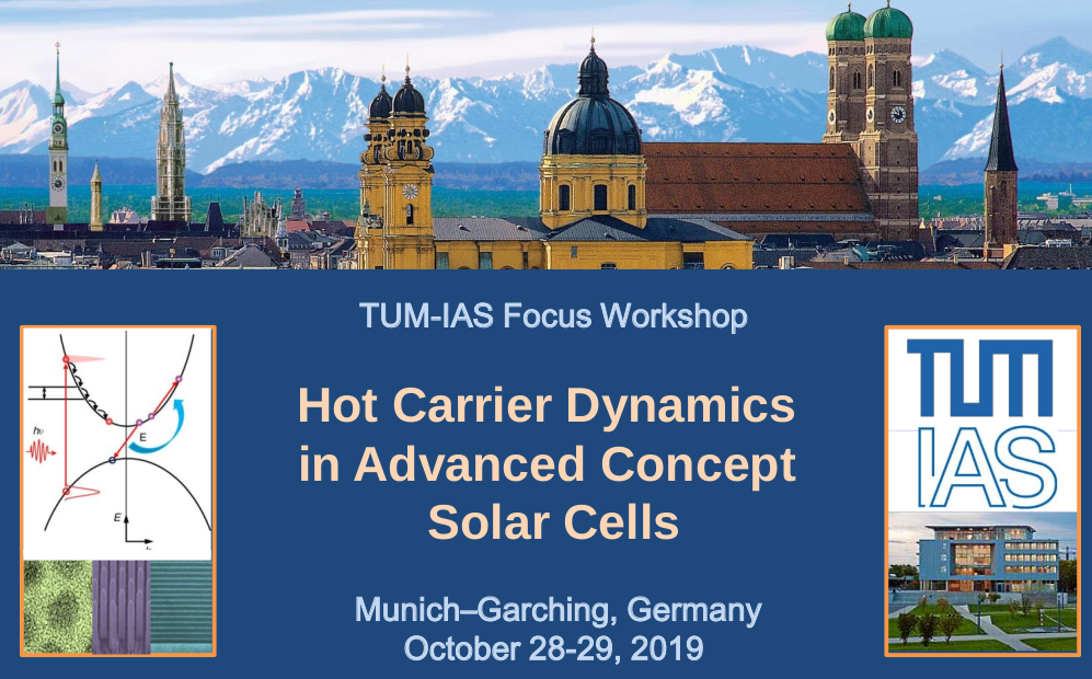
TUM-IAS Focus Workshop Oct 28th - 29th
The scope of this two-day interactive workshop is to bring together leading international scientists working in the field of “Hot carrier dynamics in advanced concept solar cells”.
A particular emphasis is placed on theoretical and experimental understanding of nonequilibrium carrier relaxation dynamics in low-dimensional semiconductor nanostructures and their exploitation for novel hot carrier type solar cells. Hereby, investigations and manipulation of ultrafast electron-phonon interactions as well as multi-exciton generation dynamics in a variety of nanostructured materials (quantum well, dots, wires, perovskites, etc.) will be discussed.
The meeting should provide a unique forum for both theoretical and experimental researchers to interact at the interface between multiscale modelling, engineering of sophisticated low-dimensional semiconductor materials, and characterization including ultrafast optical spectroscopy.
Announcement and Registration at: http://www.wsi.tum.de/hot-carrier-dynamics
6 Aug 2019
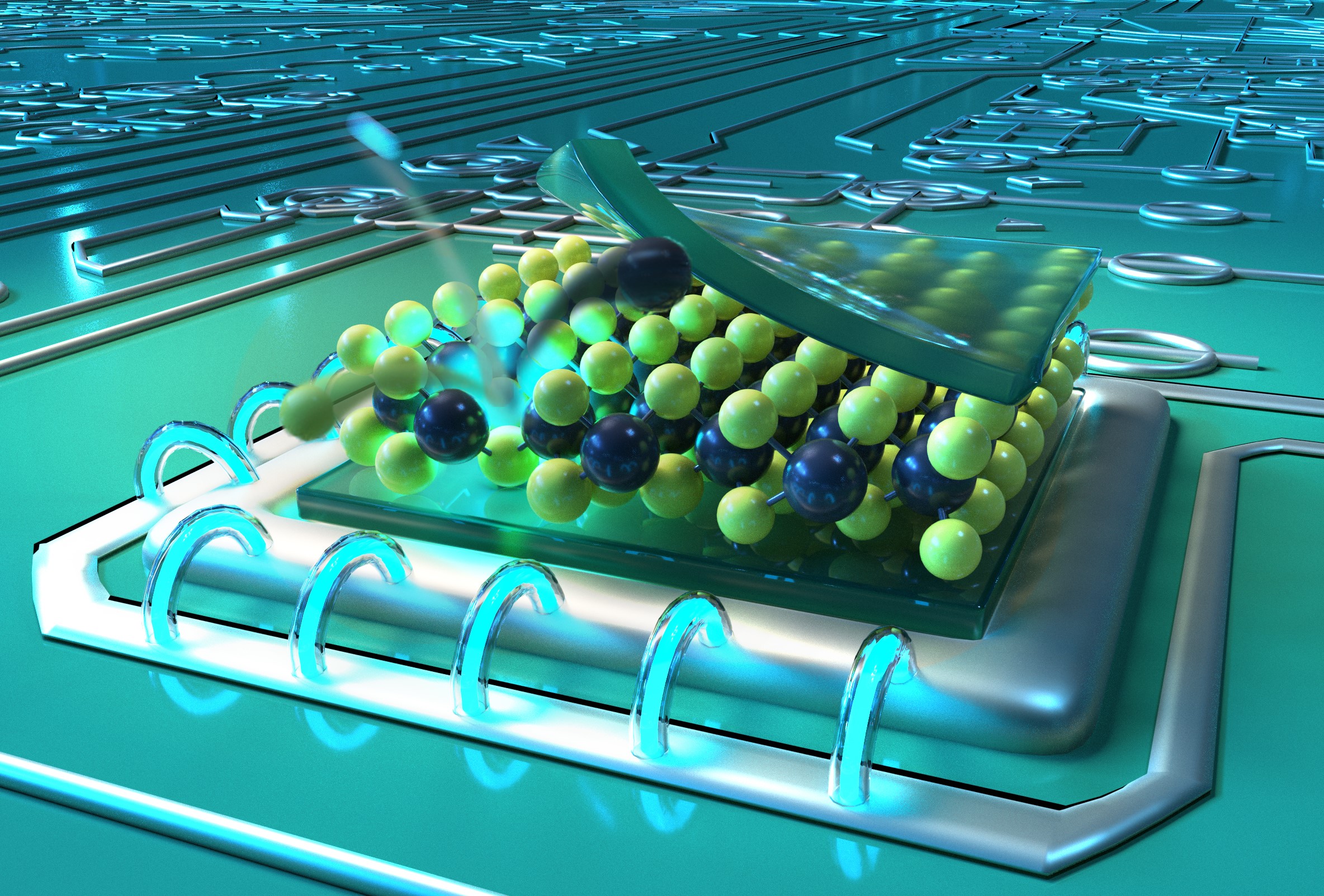
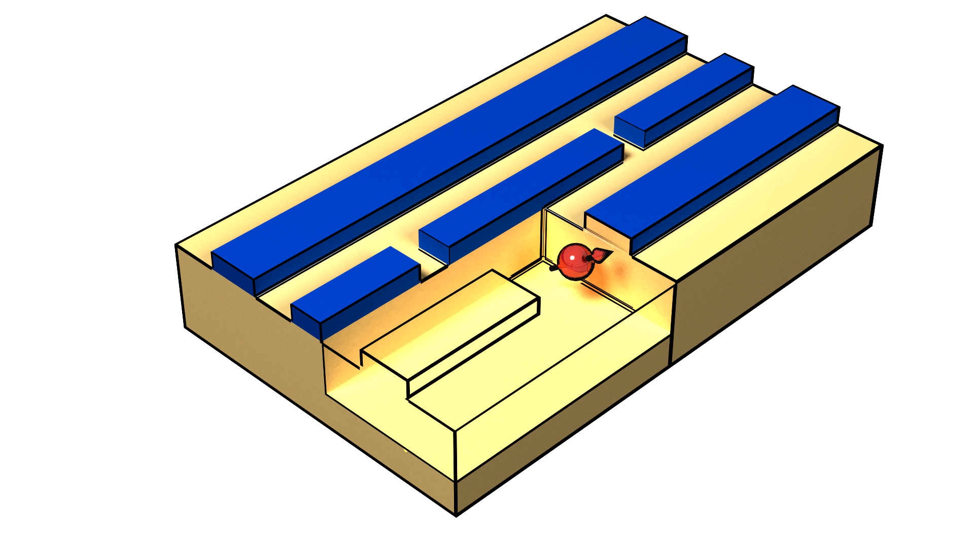
Site-selective positioning of quantum emitters
Spatially highly localized luminescent defects in solid-state materials constitute potential rudimentary building blocks for prospective quantum hardware. In a recent publication in Nature Communications the physicists Julian Klein, Prof. Jonathan Finley and Prof. Alexander Holleitner reported on a deterministic and site-selective route to incorporate single optically active defects in the atomically thin semiconductor MoS2. [1]
Previous circuits on chips rely on electrons as the information carriers. In the future, photons which transmit information at the speed of light will be able to take on this task in optical circuits. Quantum light sources, which are then connected with quantum fiber optic cables and detectors are needed as basic building blocks for such new chips. The coupling of quantum light sources to optical elements is crucially dependent on the positioning accuracy. Conventional three-dimensional materials, like silicon or diamond, which host quantum emitters suffer from spatial inaccuracies in the creation of defects. For such materials the emitters are typically embedded several nm to tens of nm from the crystal surface. In two-dimensional materials, like MoS2, the emitter is naturally restricted to an about 1 nm thick atomic layer.
Determinstic defects
For harnessing the quantum properties of defects in solids they have to be positioned site-selectively with nanometer precision in all spatial dimensions and also need to emit light at the same frequency. In this study, the researchers used a sub-nanometer focused helium ion beam in the new helium ion microscope at the Walter Schottky Institute’s Center for Nanotechnology and Nanomaterials to locally irradiate a monolayer of MoS2. Subsequent to irradiation the MoS2 is then encapsulated in the high quality insulator hBN, another material out of the exciting 2D family. The treatment results in spatially localized luminescent defects in the atomically thin semiconducting monolayer. This is the first time light sources can be generated in such a deterministic and controlled way by simultaneously maintaining nanometer accuracy. The irradiation creates defects, predominantly Mo and S vacancies, in the material that then serve as exciton traps under optical excitation. In collaboration with the theorists Michael Lorke and Matthias Florian from the University of Bremen and Richard Schmidt and Michael Knap from the TUM, a model has been developed to describe the energy states observed in the experiment. In future work, more complex light source patterns, like 2D lattices of trapped excitons are envisioned as model platform to realize Bose-Hubbard physics. Moreover, coupling to photonic elements like waveguides and cavities can now be realized with unprecedented accuracy and the high sensitivity of defects renders them for potential use as quantum sensors on the nanoscale.
Publication:
[1] Site-selectively generated photon emitters in monolayer MoS2 via local helium ion irradiation. Nature Communications, 10, 2755 (2019).
J. Klein, M. Lorke, M. Florian, F. Sigger, L. Sigl, S. Rey, J. Wierzbowski, J. Cerne, K. Müller, E. Mitterreiter, P. Zimmermann, T. Taniguchi, K. Watanabe , U. Wurstbauer, M. Kaniber, M. Knap, R. Schmidt, J.J. Finley & A.W. Holleitner
Image: Christoph Hohmann / MCQST
17 Apr 2019
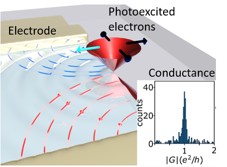
Topological quantum conductance
Crystals with symmetry-protected topological
order, such as topological insulators, promise coherent spin and charge transport
phenomena even in the presence of disorder, which
renders these topological phases promising candidates for quantum information
applications. In Physical review Letters, the
MCQST
physicists Paul Seifert, Prof. Alexander Holleitner and Dr. Christoph Kastl now demonstrated
a novel optoelectronic scheme to read-out the quantum conductance of
topological surface states. [1]
Topological
materials
The
classification of solid-state materials by the mathematical concept of topology
revolutionized condensed matter physics in the past decade, as recognized by
the Nobel prize in 2016, and lead to the discovery of a plethora of previously
unknown topological materials and quantum phases. Topological materials exhibit
surface states with unusual physical properties. For example, in so called topological
insulators (e.g. Bi2Se3) no electric current can flow through the
crystal, but the crystal surfaces conduct current almost perfectly. Intriguingly,
due to the non-trivial topology of the crystal, surface electrons moving in opposite
directions have exactly opposite spin, a property called helicity, and an
electrical current is always accompanied by a spin current in the same
direction. Unlike in other materials, the surface states are stabilized against
material imperfections or external influences by the topology of the crystal.
Therefore, these helical surface states are of interest for realizing robust spin-based
quantum information application, potentially up to room temperature.
Detecting
the surface state
For integrating
topological insulator materials into electronic circuits, it is important to be
able to read-out the surface conductance independent of a residual bulk conductance.
In previous studies, the researchers already successfully used so called scanning
photocurrent microscopy to image the effect of disorder on the surface conductance
of topological insulators. [2,3] In the current study, where they imaged the
current distribution in a field effect transistor made from the topological
insulator Bi2Se3, they made the surprising discovery that,
at the edges of the device, electrons showed a well-defined conductance which precisely
matched the conductance quantum e²/h. This finding directly showed that the
detected current was carried by a single, spin-helical surface mode, since in topologically
trivial materials two spin-degenerate modes would add up to 2e²/h.
They explain
their findings in the framework of the so-called Shockley-Ramo theory, which has
traditionally been applied to describe the signal formation
process in particle detectors. In simple words, this theory states that, in a
detector device, a moving charge creates a quasi-instantaneous macroscopic
detector current parallel to the field lines in the detector. Therefore, the
technique
does not
require a coherent transport of charge carriers all the way to the
electrodes,
in contrast to the conventional Landauer-Büttiker theory. Such optoelectronic schemes may provide a generalizable platform for
studying surface state conductance in further topological
quantum materials such
as Weyl-semimetals and quantum spin-Hall insulators.
Publications:
[1] Quantized Conductance in Topological Insulators Revealed by
the Shockley-Ramo Theorem. Phys. Rev. Lett. 122, 146804 (2019).
P. Seifert, M. Kundinger, G. Shi, X. He, K. Wu, Y. Li, A.W. Holleitner, C.
Kastl
[2] Chemical
Potential Fluctuations in Topological Insulator BiSbTe3 Films Visualized by
Photocurrent Spectroscopy. 2D Materials 2 024012 (2015).
C. Kastl, P. Seifert, X. He, K. Wu, Y. Li, A. Holleitner
[3] Local photocurrent generation in thin films of the
topological insulator Bi2Se3. Applied Physics Letters101, 25
18 Feb 2019
Valleytronics at room temperature
Essential in the development of new ultrathin information carriers is
the stabilization of the excited state, which carries the information.
The NIM physicists Prof Ursula Wurstbauer, Prof Alexander Holleitner and
Prof Alexander Högele now found a tunable method, even at room
temperature. This enables applications in so called “valleytronics”. Important feature of semiconductor materials are their energetic
properties, especially with regard to an application in optoelectronics
and information technologies. Light is used to optically generate
the information within the semiconductor crystal. Irradiation with
visible light excites a so called exciton, a mobile excited state that
propagates like a wave. So far, in practice such excited, information
carrying states of the exciton, also called valley polarization, were
stable at low temperatures (100 K, liquid nitrogen) only. The NIM physicists Professor  Ursula Wurstbauer, Professor Alexander Holleitner and Professor Alexander Högele
now clarified the underlying mechanism resulting in the depolarization
at increasing temperatures. In parallel, they developed a tunable method
to suppress that process and stabilize the valley polarization at
elevated temperatures (220 K) and even at room temperature. In Nature Communications, they present impressive results with an increased degree of valley polarization of 20 % and more. Ursula Wurstbauer, Professor Alexander Holleitner and Professor Alexander Högele
now clarified the underlying mechanism resulting in the depolarization
at increasing temperatures. In parallel, they developed a tunable method
to suppress that process and stabilize the valley polarization at
elevated temperatures (220 K) and even at room temperature. In Nature Communications, they present impressive results with an increased degree of valley polarization of 20 % and more.
Efficient single layers
Molybdenum disulfide (MoS2)
is a member of the emerging material class of two-dimensional
transition metal dichalcogenides. Its properties include stability in
the presence of oxygen, water and diluted acids as well as a high
melting temperature. All making the semiconductor an ideal candidate in
the development of new information technology devices. Additionally, even single-layered MoS2
is very sensitive to light-dependent processes. So called valley
degrees of freedom, specific energy levels within the lattice structure,
allow for valley-specific selective optical excitation and local
increase of the charge density. Stabilization of the valley polarization
is prerequisite for lossless devices and their commercial
applicability.
Stabilization of excited states
Theoretically, the valley
polarization should be stable after the excitation with light at room
temperature, in the practice this was not the case. The physicists now
could elucidate the nearly-breakdown of the polarization of excitons in
semiconductor crystals is due to the coupling of excitons to specific
lattice oscillations, so called phonons. “One could picture the
depolarization process, especially at elevated temperatures, as the
coupling of around themselves rotating excitons and phonons,” Ursula
Wurstbauer explains, “and this movement is propagating like a wave front
on a water.” The coupling of the excitons to longitudinal optical
phonons is called Fröhlich exciton-phonon interaction and enhances the
depolarization. “Doping of the semiconductor with electrons can
longlastingly suppress that coupling,” Wurstbauer describes the basis of
the new strategy to stabilize the valley polarization.“Mechanistically, the added electrons shield the electrical field
induced by lattice oscillations. Hence, the coupling of excitons is
suppressed,” the physicist further explains, “Comparing the system to a
water again, we fill the lake with electrons and thereby smooth the
oscillations of the electric field. The scattering of a valley-polarized
exciton on phonons after excitation with light is suppressed.” The
gained basic understanding of the depolarization mechanism enabled the
scientists to develop a strategy to stabilize the valley polarization.
Doping of the semiconductor with electrons makes the depolarization
process tunable. Another extra of their method is the reduction of
scattering due to lattice imperfections and disorder.
Publication:
Tuning the Fröhlich exciton-phonon scattering in monolayer MoS2. Miller
B, Lindlau J, Bommert M, Neumann A, Yamaguchi H, Holleitner A, Högele
A, Wurstbauer U. Nature Communications 10, 807 (2019), DOI: 10.1038/s41467-019-08764-3
30 Jan 2019
Fundamental work on dislocation-mediated effects on thermal transport published in Nature Materials
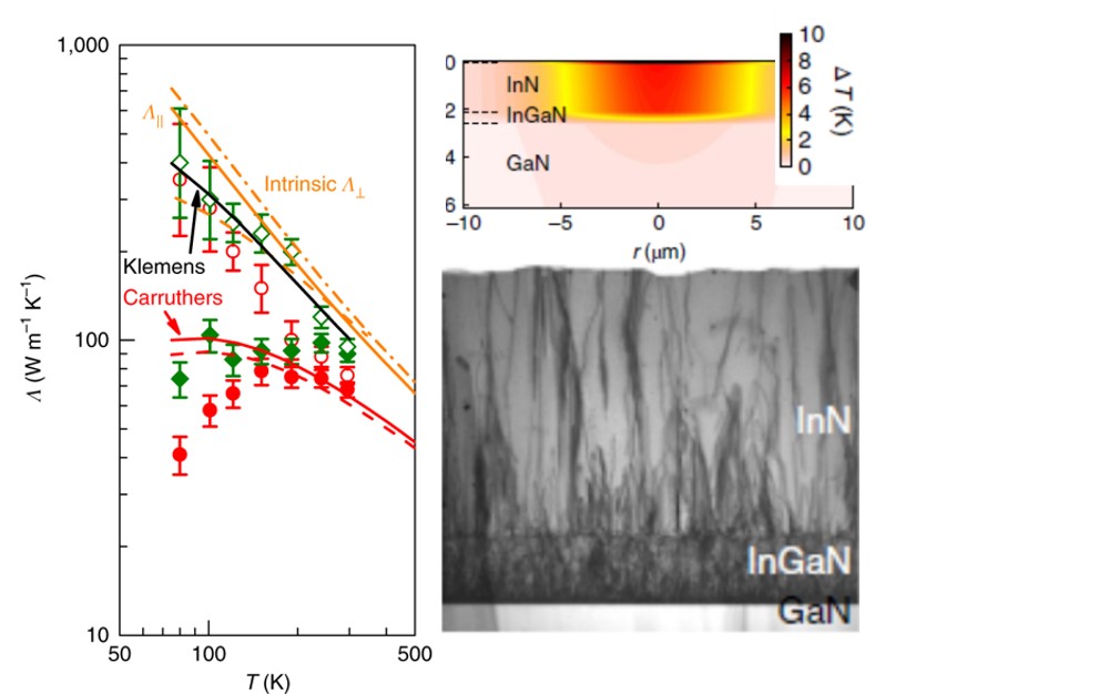
Extended defects such as dislocations are common in technologically important III-V semiconductors, and affect heat dissipation, for example, in nitride-based high-power electronic devices. For decades, dislocations were predicted to induce anisotropic heat transport depending on their direction, however, experimental observation has been still lacking.
In a well-concerted collaboration between teams at the National University of Singapore (NUS), Oak Ridge National Laboratory (ORNL, USA) and WSI-TUM, highly oriented threading dislocation (TD) arrays were designed in few-µm thick, epitaxial InN (indium nitride) films for which the strong thermal transport anisotropy was measured for the first time using time-domain thermoreflectance. The results published in B. Sun, et al, Nature Materials 18, 136 (2019) show that the cross-plane thermal conductivity is almost 10-fold higher than the in-plane thermal conductivity for state-of-the-art TD densities of ~1010/cm2. With enhanced understanding of dislocation-phonon interactions obtained here, this work fuels the developments for directed heat dissipation in the thermal management of diverse device applications.
https://www.nature.com/articles/s41563-018-0250-y
15 Jan 2019
Best Poster Award at MRS Fall Meeting for Thomas Stettner and Daniel Ruhstorfer
Thomas Stettner and Daniel Ruhstorfer, both PhD students at the Walter Schottky Institute share a Best Poster Award that was recently awarded at the MRS Fall Meeting 2018 held by the Materials Research Society in Boston, USA (Nov. 25-30, 2018). The MRS Fall Meeting is one of the largest international conferences for materials research with over 50 symposia and ca. 6000 attendees annually.
The awardees received their prize for their contribution entitled “GaAs-AlGaAs core-shell nanowire lasers on silicon” which was presented in the Symposium “Nanowires and Related 1D Nanostructures – New Opportunities and Grand Challenges”. Thomas Stettner and Daniel Ruhstorfer are both students supervised by PD Dr. Gregor Koblmüller at the Semiconductor Quantum Nanosystems Chair of Prof. Jonathan Finley at WSI.
23 Nov 2018
The institute mourns for Prof. Markus-Christian Amann. He passed away unexpectedly on 23. Nov. 2018.
Markus-Christian
Amann
Prof.
Markus-Christian Amann passed away unexpectedly on 23.11.2018 at the age of 67
years. Until April 2018 he was Full Professor for Semiconductor Technology at
TUM and Director of the Walter Schottky Institut.
After
completing his studies at the Faculty for Electronic and Computer Engineering of
TUM, Markus-Christian Amann joined the research laboratories of Siemens AG in
Munich in 1981 where he remained until 1994, rising to lead the department for Semiconductor
Research & Optoelectronics. Subsequently, he accepted a call to a Chair for
Technical Electronics at the University of Kassel where he taught and
researched until 1997. In 1997 he received a call to the TUM, where he held the
chair for Semiconductor Technology at the Walter Schottky Institut until his
retirement in April 2018.
Markus-Christian
Amann was a very well-known and highly-respected figure in the international
scientific community. He performed
groundbreaking work in the field of III-V semiconductor optoelectronic devices,
including vertical cavity surface emitting lasers - key components for high
bandwidth optical data communication systems and optical metrology and sensing
systems. His work is documented by more than 500 scientific publications,
patents and conference proceedings that also formed the intellectual basis for
the successful launch of several start-up companies.
Markus-Christian
Amann received many prizes and accolades for his scientific work. Specific examples
include the Karl-Heinz-Beckurts prize in 2007, from the Foundation bearing the
same name and a nomination to be Fellow of the IEEE Society in 2009. Beyond his
research, he made major contributions to scientific administration being
referee for many leading international scientific journals, as a committee
member for the Germany Science Foundation, as vice Dean and Dean of the faculty
for Electronic and Computer Engineering and as Managing Director of the Walter
Schottky Institut.
Martin Stutzmann
31 Oct 2018
A new hybrid device for renewable electricity and fuels from sunlight
Our group has developed and demonstrated a new device that allows for simultaneous production of electricity and chemical fuels from sunlight. The new device, called a hybrid photoelectrochemical and photovoltaic (HPEV) cell, overcomes central challenges in the area of artificial photosynthesis, as described in our recent paper in Nature Materials: G. Segev, J.W. Beeman, J.B. Greenblatt, & I.D. Sharp, Nature Materials (2018). A press release describing this exciting advancement can be found here.
27 Sep 2018
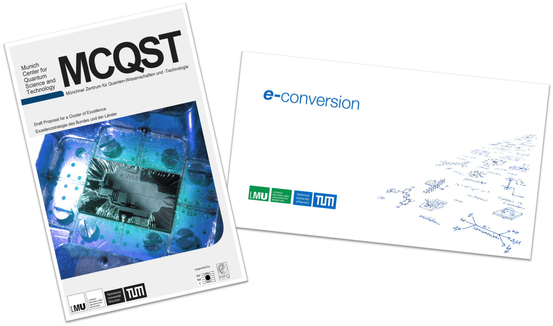
WSI celebrates successes in Excellence Initiative !
Walter Schottky Institute scientists were thrilled with the great news on 27.09.18 that Technical University of Munich was again successful in the extremely competitive Excellence Initiative organised by the Federal and Regional Governments. From Jan 2019 onwards, research groups from WSI led by Profs. Brandt, Finley, Holleitner, Sharp and Stutzmann will be strongly involved in two DFG Clusters of Excellence for the next seven years. After a two-step selection procedure lasting over 18 months, a high-level international committee approved two clusters for funding with participation of WSI groups - e-Conversion and MCQST (Munich Center for Quantum Science and Technology)
e-CONVERSION (Finley, Holleitner, Sharp, Stutzmann)
The e-conversion Cluster of Excellence explores ways to deliver a stable, efficient and sustainable supply of energy by combining nanoscience with energy sciences. This cluster focuses on the energy conversion processes of different technologies – from photovoltaics through (photo-)electrocatalysis to battery technologies. To date, inadequate control of these processes in nanomaterials and at relevant interfaces has led to resistance, recombination losses or overvoltage, all of which compromise the efficiency of power generation. e-conversion will study the basic mechanisms of energy conversion with a time resolution in the femtosecond range. The findings will enable scientists to design and synthesize energy materials with atom-scale precision. The cluster will build an electron microscopy center in order to characterize the materials. Alongside WSI scientists, e-conversion will involve many TUM and LMU groups, the Max Planck Institutes for Chemical Energy Conversion (Mülheim/Ruhr) and for Solid State Research (Stuttgart).
MUNICH CENTER FOR QUANTUM SCIENCE AND TECHNOLOGY (Brandt, Finley, Holleitner)
Breakthroughs in quantum mechanics have inspired everyday technologies such as microchips, computers and lasers. Quantum mechanics describes the physical properties of the smallest particles, and work in this area revolutionized the world of science in the 20th century. A technological leap forward is currently taking place known as “Quantum 2.0”. It is based on the use of superposition and entanglement of quantum states. The number of potential applications is huge, with ultra-high-performance quantum computers and secure quantum communication systems being just two examples. The objective of the Munich Center for Quantum Science and Technology is to further the scientific understanding of quantum mechanics phenomena and thus advance basic components, materials and concepts for quantum technologies. Interdisciplinary research extends from the analysis of entanglement in multiparticle systems to quantum chemistry, astronomy and precision metrology. Alongside WSI Scientists, MCQST will involve many TUM and LMU groups working besides scientists from the Max Planck Institute of Quantum Optics, the Walther Meißner Institute of the Bavarian Academy of Sciences and Humanities and the Deutsches Museum.
27 Jun 2018
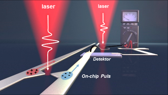
Closing the gap: On the road to Terahertz electronics
Asymmetric plasmonic antennas deliver femtosecond pulses for fast optoelectronics
A team headed by the TUM physicists Alexander Holleitner and Reinhard Kienberger has succeeded for the first time in generating ultrashort electric pulses on a chip using metal antennas only a few nanometers in size, then running the signals a few millimeters above the surface and reading them in again a controlled manner. The technology enables the development of new, powerful terahertz components.
Classical electronics allows frequencies up to around 100 gigahertz. Optoelectronics uses electromagnetic phenomena starting at 10 terahertz. This range in between is referred to as the terahertz gap, since components for signal generation, conversion and detection have been extremely difficult to implement.
The TUM physicists Alexander Holleitner and Reinhard Kienberger succeeded in generating electric pulses in the frequency range up to 10 terahertz using tiny, so-called plasmonic antennas and run them over a chip. Researchers call antennas plasmonic if, because of their shape, they amplify the light intensity at the metal surfaces.
Asymmetric antennas
The shape of the antennas is important. They are asymmetrical: One side of the nanometer-sized metal structures is more pointed than the other. When a lens-focused laser pulse excites the antennas, they emit more electrons on their pointed side than on the opposite flat ones. An electric current flows between the contacts – but only as long as the antennas are excited with the laser light.
"In photoemission, the light pulse causes electrons to be emitted from the metal into the vacuum," explains Christoph Karnetzky, lead author of the Nature work. "All the lighting effects are stronger on the sharp side, including the photoemission that we use to generate a small amount of current."
Ultrashort terahertz signals
The light pulses lasted only a few femtoseconds. Correspondingly short were the electrical pulses in the antennas. Technically, the structure is particularly interesting because the nano-antennas can be integrated into terahertz circuits a mere several millimeters across.
In this way, a femtosecond laser pulse with a frequency of 200 terahertz could generate an ultra-short terahertz signal with a frequency of up to 10 terahertz in the circuits on the chip, according to Karnetzky.
The researchers used sapphire as the chip material because it cannot be stimulated optically and, thus, causes no interference. With an eye on future applications, they used 1.5-micron wavelength lasers deployed in traditional internet fiber-optic cables.
Holleitner and his colleagues made yet another amazing discovery: Both the electrical and the terahertz pulses were non-linearly dependent on the excitation power of the laser used. This indicates that the photoemission in the antennas is triggered by the absorption of multiple photons per light pulse.
"Such fast, nonlinear on-chip pulses did not exist hitherto," says Alexander Holleitner. Utilizing this effect he hopes to discover even faster tunnel emission effects in the antennas and to use them for chip applications.
Figure:
Pulses of femtosecond length from the pump laser (left) generate on-chip electric pulses in the terahertz frequency range. With the right laser, the information is read out again. (Image: Christoph Hohmann / NIM, Holleitner / TUM)
Publication:
Towards femtosecond on-chip electronics based on plasmonic hot electron nano-emitters.
C. Karnetzky, P. Zimmermann, C. Trummer, C. Duque-Sierra, M. Wörle, R. Kienberger, A. Holleitner; Nature Communications June 25, 9, 2471 (2018).
More information:
The experiments were funded by the European Research Council (ERC) as part of the "NanoREAL" project and the DFG Cluster of Excellence "Nanosystems Initiative Munich" (NIM).
Contact:
Prof. Dr. Alexander Holleitner
Walter Schottky Institute / Department of Physics
Center for Nanotechnology and Nanomaterials
Technical University of Munich
Am Coulombwall 4a, 85748 Garching, Germany
Tel: +49 89 289 11575
E-Mail: holleitner@wsi.tum.de
Web: https://www.wsi.tum.de/sub_group.php?group=Holleitner
Prof. Dr. Reinhard Kienberger
Physik-Department E11
Technical University of Munich
James-Franck-Str. 1, 85748 Garching, Germany
Tel: +49 89 289 12840
E-Mail: reinhard.kienberger@tum.de
Web: http://www.groups.ph.tum.de/e11
13 Feb 2018
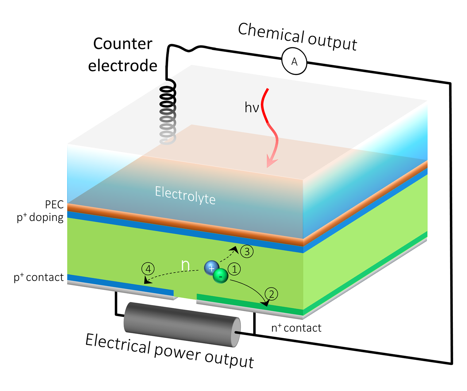
Understanding life cycles of charge carriers in functional photoelectrodes
The next generation of solar energy conversion systems requires the discovery of semiconductors with properties tailored to their desired function. In this pursuit of such new materials, detailed understanding of optoelectronic properties, driving forces for charge separation and extraction, and loss mechanisms that limit device performance is essential for achieving high efficiencies. However, few experimental methods are available for direct characterization of these fundamental processes in artificial photosystems that are designed to convert sunlight into fuels. To overcome this gap, researchers are developing new methods for operando characterization of photoelectrochemical systems comprising illuminated and electrified semiconductors in aqueous environments that are incompatible with many traditional spectroscopic tools.
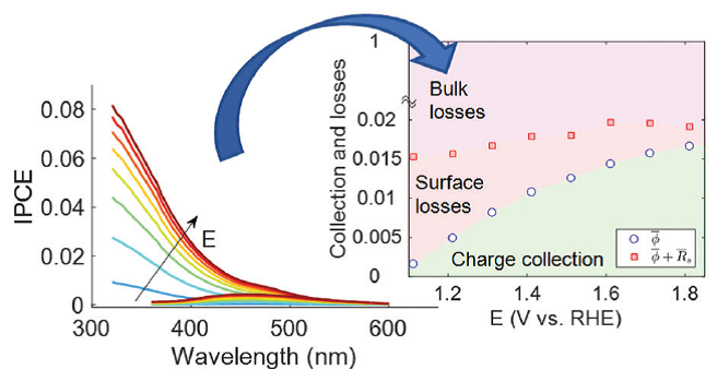
Reporting in the journal Energy and Environmental Science, an international team of scientists working at the Walter Schottky Institute and the Lawrence Berkeley National Laboratory, led by Ian Sharp, have developed a new approach for identification and quantification of photocarrier transport and efficiency loss mechanisms in operating photoelectrodes with nanometer depth resolution. In their work, they applied this method to a newly identified and thus poorly understood semiconductor, copper vanadate, which possesses an ideal bandgap for photoelectrochemical energy conversion. In doing so, they provided key insights into charge transport and loss mechanisms that are ubiquitous in a broad range of recently identified transition metal oxide materials. Such details regarding photocurrent generation and recombination at operating semiconductor/electrolyte junctions not only provide guidance to future material discovery efforts, but also motivate strategies for nanostructuring photoelectrodes, engineering interfaces, and integrating catalysts. More broadly, this work represents a significant leap forward in the ability to understand the key aspects of functional photosystems by probing the nanoscale life cycles of charge carriers in advanced materials interacting with complex environments.
Quantification of the loss mechanisms in emerging water splitting photoanodes through empirical extraction of the spatial charge collection efficiency
G. Segev, C.-M- Jiang, J.K. Cooper, J. Eichhorn, F.M. Toma & I.D. Sharp, Energy Environ. Sci. (2018) doi: 10.1039/C7EE03486E.
17 Jan 2018
ERC Consolidator Grant for Gregor Koblmüller
A Consolidator Grant was awarded by the European Research Council (ERC) in its latest funding round to PD Dr. Gregor Koblmueller (WSI & Physics Department, TU Munich). Gregor Koblmueller received the award for his project QUANtIC which focuses on novel "Quantum Nanowire Integrated Photonic Circuits". Consolidator Grants are among the largest and most prestigious single-PI awards within the European research community and are given to outstanding researchers who have demonstrated independent and highly creative research. The award is worth nearly 2 Mio € and allows the recipient to conduct cutting-edge research on the proposed topic over the next five years. Gregor Koblmueller (picture) will use the Consolidator Grant to create and explore new links between semiconductor nanowires with precisely tailored quantum electronic properties and nanoscale integrated photonic circuits. The vision is to enable thereby highly deterministic and site-selectively integrated nanoscale coherent light sources, such as efficient nanolasers and single photon emitters, direcly on photonic and quantum photonic hardware. These integrated light sources are expected to provide novel grounds for future applications in the fields of on-chip light processing, quantum communication, as well as lab-on-chip sensing. Gregor Koblmueller has been active at WSI for many years where he is leading the Semiconductor Quantum Nanomaterials group. More information on his research activities can be found at www.wsi.tum.de/koblmueller 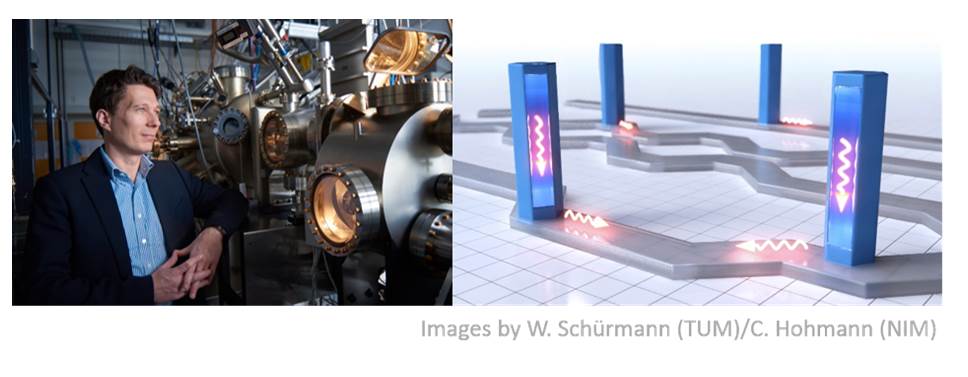
16 Jan 2018
Light-steering of spin-polarized currents in topological insulators
Topological insulators are a fascinating group of materials. A spin-polarization occurs, as soon as an electric current flows in the material. WSI scientist Prof Dr Alexander Holleitner and his cooperation partners measured this now for the first time optically at room temperature. In particular, they succeeded to steer spin-polarized currents towards the edges by a circularly polarized light beam and to read-out the electron spin-polarization at the facets of the circuits.
Topological insulators
About ten years ago, scientists discovered a group of materials called "topological insulators" with unusual electronic properties. The interior acts as an insulator, but the surface conducts electricity better than average. The group of the NIM physicist Professor Alexander Holleitner (weblink: www.nanoptronics.de) has succeeded to guide electrons with opposite magnetization, in short spin-polarization, towards the opposite edges of a topological insulator. Key feature is that no external magnetic field is needed to generate this phenomenon. The opposite spin-polarization rather derives from an effect called spin-orbit-coupling. The direct coupling between the electron’s spin and the direction of the electron motion allows its manipulation. The physicists found this effect to be reversible. By inducing a certain magnetization with polarized light, they can control the electric current at the sample’s edges. Their results are presented in the latest issue of Nature Communications (Weblink: https://www.nature.com/articles/s41467-017-02671-1).
The best-known representatives of three-dimensional topological insulators are heavy metal alloys, such as bismuth selenide or bismuth telluride. Scientists assign the exceptional electronic properties to be a phenomenon of quantum physics: the so-called spin-Hall-effect. One observes that all electrons moving in the surface layers have a well-defined spin. In doing so, they differ "topologically" from electrons inside the materials. The direction of the surface currents is directly linked to the electron spin. In such spin-orbit materials, an electron with positive spin always flows in the opposite direction compared to an electron with negative spin.
Holleitner and colleagues now made the stunning discovery that this also holds for the material’s interior, if it is electrically conducting. When a current flows through the topological insulator, electrons with opposite spin move in opposite directions and accumulate at the topological edges of the material. The imbalance in the spin distribution results in a magnetization of the surface states.
Spin-polarized currents at the facets
In conventional conductors, electric currents are always carried by electrons with an arbitrary spin-orientation. In topological insulators, however, the direct coupling between the electron’s spin and the direction of movement allows a particular control of the electrons without the necessity of a sophisticated magnetic field or magnetic materials.
"Such control of the electronic spin is the basic requirement for the realization of so-called spin-based electronics.", explains first author Paul Seifert, who designed and carried out the experiments. The scientists hope that this technology will be applied in the development of more powerful computers or the secure encryption of data.
Measurements with polarized light
Very small electric currents and their magnetization can be directly detected with polarized light. In the actual experiment, they contact a topological insulator between two electrodes and excite the material with a circularly polarized laser. By choosing the correct polarization, they can induce a magnetization in the material, as electrons with different spin can be excited selectively.
Through a circuit, the scientists are able to track how a spin-polarized current at the edges of the topological insulator changes when they change the polarization of the light. In addition, the scientists observed the local magnetization of the topological insulator to change the polarization of the reflected light. Thus, they were able to directly detect the magnetization or spin polarization generated by the current flow.
Funding:
The experiments are funded by the Deutsche Forschungsgemeinschaft within DFG Projects 3324/8-1 of the SPP 1666 “topological insulator“ and the excellence cluster “Nanosystems Initiative Munich“ (NIM). The co-authors Dr. K. Vaklinova, Prof. K. Kern and Dr. M. Burghard work at the Max Planck Institute for Solid State Research in Stuttgart. Co-author Sergey Ganichev works at the Terahertz Center of the University of Regensburg.
Publication:
Spin Hall photoconductance in a three-dimensional topological insulator at room temperature. Paul Seifert, Kristina Vaklinova, Sergey Ganichev, Klaus Kern, Marko Burghard und Alexander W. Holleitner. Nature Communications
Contact:
Prof Dr Alexander Holleitner
Walter Schottky Institute and Physics-Department
Center for Nanotechnology and Nanomaterials
Technische Universität München
Am Coulombwall 4a
85748 Garching
Germany
Tel: 089/289-11575
E-Mail: holleitner@wsi.tum.de
Web: Holleitner Group
Picture:
Helicity-dependent edge conductance.
18 Oct 2017
Quantum sensing of GHz frequency signals
Quantum sensors can detect signals at much higher frequencies than previously thought. This is a finding that our quantum sensing group reports in Nature Communications this week. A novel sensing scheme based on this insight could lead to a new generation of quantum devices, such as detectors for single microwave photons.
Nature Communications 8, 964 (2017)
01 Sept 2017
WSI Welcomes Prof. Ian Sharp
We extend a warm welcome to our new colleague, Prof. Ian Sharp, who joined the Walter Schottky Institute on September 1st, 2017. Prof. Sharp, who holds the Chair for Experimental Semiconductor Physics at the Technical University of Munich, pursues research into functional materials and interfaces for renewable energy conversion. His interests include development of artificial photosystems that convert sunlight into chemical fuels, synthesis and characterization of new semiconductors and nanosystems, and investigation of physical and chemical mechanisms of energy conversion.
Before coming to the Technical University of Munich, Prof. Sharp was a Staff Scientist at the Lawrence Berkeley National Laboratory. While there, he served as Thrust Lead at the Joint Center for Artificial Photosynthesis and, in 2016, was recipient of the prestigious U.S. Department of Energy Early Career Award. From 2007 to 2011, Dr. Sharp was a post-doctoral fellow in the group of Prof. Stutzmann, initially as an Alexander von Humboldt Fellow and later as a Carl von Linde Junior Fellow of the TUM Institute for Advanced Study.
It is a pleasure to welcome Ian Sharp back to the Walter Schottky Institute!
10 Aug 2017
Best Poster Awards for Ganpath Veerabathran and Alexander Andrejew at iNOW 2017
Ganpath Veerabathran and Alexander Andrejew, both doctoral candidates from Prof. Amann's group (E26) at the WSI, received Best Poster Awards at the International Nano-Optoelectronics Workshop (iNOW) in Tianjin, Qian’an & Chengde, China (2017). Ganpath Veerabathran's poster titled "GaSb-based vertical-cavity surface-emitting lasers at 4 μm using type-II quantum wells" was awarded the 1st place out of 42 posters. The prize consists of a certificate and carries a value of 400 USD. Alexander Andrejew's poster titled “Electrically pumped mid-infrared vertical-cavity surface-emitting lasers emitting at 3 μm” was selected for the ‘Honorary mention’ award.
27 Jun 2017
Best Poster Award at Nanowire Week for Jochen Bissinger
Jochen Bissinger, PhD student at the Walter Schottky Institut was awarded with the Best Poster Award at Nanowire Week 2017 in Lund Sweden (29th May - 2nd June, 2017). The Nanowire Week (combined 10th Nanowire Growth Workshop and 9th Nanowires Workshop) is nowadays one of the most significant international conferences for semiconductor nanowire-related research with over 300 participants annually.
Selected from 180 poster presentations Jochen Bissinger received the Best Poster prize for his contribution entitled "Simulation of monolithically integrated Ga(Al)As-InGaAs core-multishell nanowire lasers on silicon waveguides". Jochen Bissinger is a member of the WSI Nanowire Group and is co-supervised by Dr. Gregor Koblmüller, Dr. Michael Kaniber, and Prof. Jonathan Finley. His PhD thesis work is performed in collaboration with the Electrical Engineering Department at TUM and is funded by the International Graduate School of Science and Engineering (TUM-IGSSE).
15 Mar 2017
Dr. Kai Müller admitted to the “Junges Kolleg” of the Bavarian Academy of Sciences
Recently, Dr. Kai Müller a subgroup leader at the chair E24 (Prof. Finley) was admitted to the “Junges Kolleg” of the Bavarian Academy of Sciences and Humanities. The “Junges Kolleg” was found in 2010 in order to support promising junior scientist and foster interdisciplinary research. It consists of 20 young scientists, carrying our research across all disciplines and all universities / research institutions in Bavaria. This year, 5 researchers out of 60 highly qualified applicants were admitted. More information can be found here: Press release from BAdW Homepage of the “Junges Kolleg”
27 Feb 2017
Two-photon pulses from a single two-level system
Sources of non-classical states of light are key components needed for future quantum photonic technologies such as intrinsically secure communication, distributed quantum information processing and precision metrology. By far the most commonly non-classical light sources investigated to date can generate individual quanta of light - single photons. A well-established technique to generate single photons on-demand involves using short laser pulses to resonantly excite an individual two-level quantum system, such as an atom or semiconductor quantum dot. A team of scientists lead by Dr. Kai Müller (E24 / Prof. J. Finley) have now discovered that resonantly driven two-level systems can also act as sources of two-photon pulses when excited by laser pulses having specially tailored properties. The work has been performed in the framework of a collaboration between the WSI and the group of TUM-IAS Hans Fischer senior fellow Prof. J. Vuckovic at Stanford University and is also supported financially by the BMBF and the DFG via the Nanosystems Initiative Munich. The paper is published in Nature Physics and can be viewed at: Emission of two-photon pulses from a quantum two-level system
Kevin A. Fischer, Lukas Hanschke, Jakob Wierzbowski, Tobias Simmet, Constantin Dory, Jonathan J. Finley, Jelena Vuckovic and Kai Müller
Nature Physics (2017) doi:10.1038/nphys4052
05 Aug 2016
Best Poster Award at iNow 2016 for Hannes Schmeiduch
The contribution "Selective Area Epitaxy and Growth on Patterned Surfaces of Indium Phosphide using LP-MOVPE for MIR-QCL" presented by Hannes Schmeiduch at International Nano-Optoelectronics Workshop 2016 (iNow) in München and Würzburg, has been award the 3rd "Best Poster Award" out of 38 posters. The research team consists of researchers from Chair E26 at the Walter Schottky Insitut/TU München (H. Schmeiduch, F. Demmerle, S. Saller, S. Sprengel, W. Oberhausen, R. Meyer, and M.-C. Amann). We especially thank Mr. Demmerle for his encouragement.
27 Jul 2016
Best Poster Award for "Few-QD nanolaser" at PECS-XII
The contribution "A few-emitter solid-state multi-exciton laser" presented by Michael Kaniber at "The 12th International Symposium on Photonic and Electromagnetic Crystal Structures (PECS-XII)" in York, UK, has been selected out of 40 posters for a runner-up poster award. The research team consists of researchers from Chair E24 at the Walter Schottky Insitut/TU München (S. Lichtmannecker, T. Reichert, M. Blauth, Dr. M. Kaniber, and Prof. J. J. Finley) and from the Solid-state Theory-group at Universität Bremen (Dr. M. Florian, Dr. C. Gies, and Prof. F. Jahnke). We thank the whole team for their efforts and great work! Congratulations!
13 Jul 2016
Best Poster Award at HeFIB for Julian Klein
Julian Klein, Ph.D student at the Walter Schottky Institut, has very recently been awarded with the 1st price for his Poster contribution at the HeFib, "1st International Conference on Helium Ion Microscopy and Emerging Focused Ion Beam Technologies", in Luxembourg (June 8-10). His poster entitled "Optical properties of 2D materials exposed to helium ions" combines novel methods of nanostructuring performed by a helium ion microscope applied to semiconducting atomically thin 2D materials. Julian Klein is supervised by Dr. Michael Kaniber, Dr. Ursula Wurstbauer, Prof. Jonathan Finley and Prof. Alexander Holleitner in the Integrated Quantum Photonics Group at the Walter Schottky Institut. He investigates optical properties of atomically thin 2D materials in combination with plasmonic nanostructures.
04 Jul 2016
CSW 2016 Best Paper Award for Bernhard Loitsch
Bernhard Loitsch, PhD student at the Walter Schottky Institut won the Best Student Paper Award at
the international Compound Semiconductor Week 2016 (CSW2016) held in Toyama (Japan). CSW2016 is
a joint venue for the 43rd International Symposium on Compound Semiconductors (ISCS) and the
28th International Conference on Indium Phosphide and Related Materials (IPRM) and a premier
forum for science, technology and applications in all areas of compound semiconductors.
He gave an oral presentation entitled “Quantum Confinement Phenomena in Ultrathin
GaAs Nanowires”. Based on an evaluation of the quality of abstracts and oral
presentations by a panel of international experts, only three papers were selected from a
large number of eligible contributions. Bernhard Loitsch is a student in the Nanowire
Group led by Dr. Gregor Koblmüller at the Semiconductor Quantum Nanosystems Chair
(Prof. Finley) and investigates growth, structure-property correlations, and advanced optical
properties in III-V semiconductor nanowire systems in his Ph.D. thesis work.
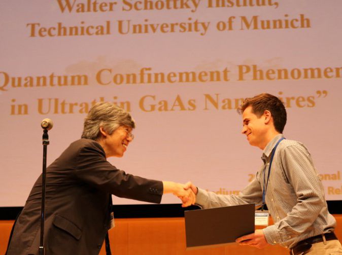
Foto: CSW2016
14 Jun 2016
Poster Award at 10th IGSSE Forum in Raitenhaslach
The “Nanowire lasers”-team (IGSSE Project 9.08) working at WSI-TUM (Chair Prof. J. J. Finley) and TUM-EE (Chair Prof. P. Lugli) were recently awarded the Best Poster Award at the 10th IGSSE Forum held in Raitenhaslach (June 1-4). The PhD students Thomas Stettner, Jochen Bissinger, Armin Regler and the Project Team Leader Dr. Michael Kaniber won the 3rd prize with their contribution entitled “Nanowire lasers for information technologies and sensing”. This collaborative IGSSE Project brings together students from the Physics Department/Walter Schottky Institut as well as from the Faculty of Electrical and Computer Engineering and explores the potential of III-V semiconductor nanowires as coherent light sources for applications in future optical on-chip and interconnects communication.
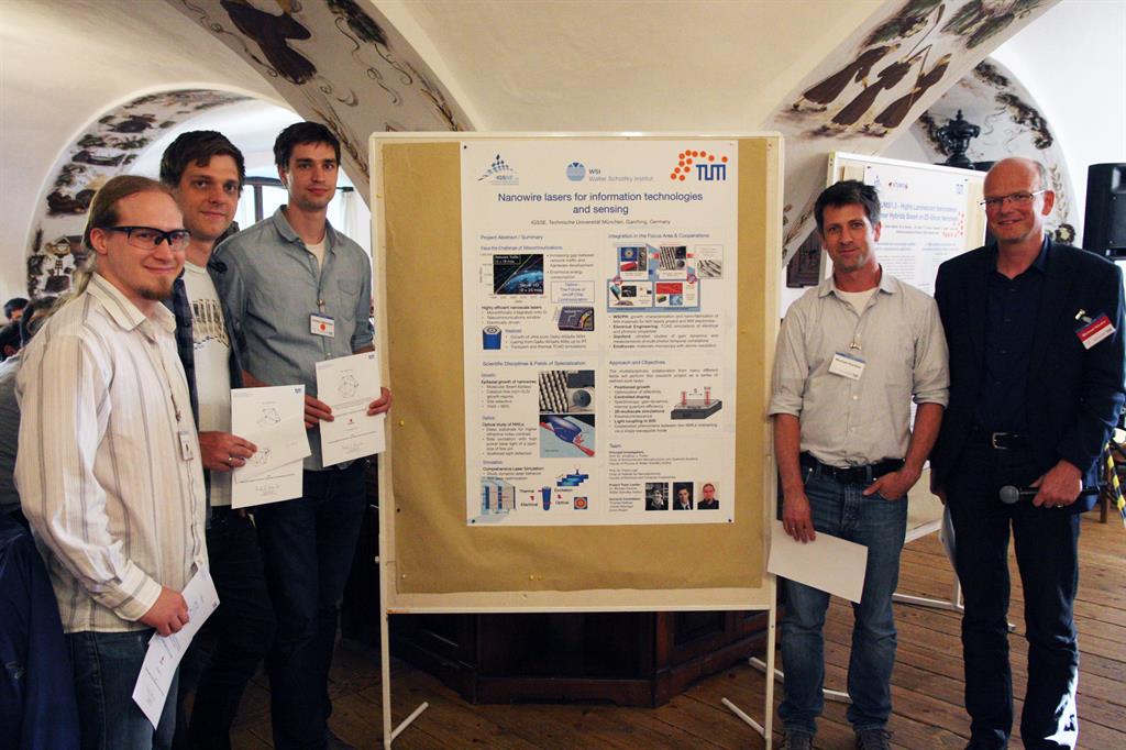
21 Mar 2016
IBM Ph.D. Fellowship for Bernhard Loitsch
Bernhard Loitsch, Ph.D. student at the Walter Schottky Institut, has received the prestigious IBM Ph.D Fellowship award. This is the second successful nomination after an initial award in 2014, which was followed by an ongoing scientific collaboration and mentorship with Dr. Heike Riel, IBM Fellow and Manager of the Nanoscale Electronics group at IBM Research – Zurich. The IBM Ph.D. Fellowship Awards Program is an intensely competitive worldwide program, which honors exceptional Ph.D. students with a $20.000 stipend for one academic year. Bernhard Loitsch is a Ph.D. student supervised by Dr. Gregor Koblmüller and Prof. Jonathan Finley in the Quantum Nanomaterials Group at the Walter Schottky Institut. He investigates the epitaxial growth of GaAs-based nanowire heterostructures as well as their optical and electrical properties.
07 Jan 2016
Arnold Sommerfeld Prize 2015 for Gregor Koblmueller!
Our congratulations to Gregor Koblmueller on being awarded the Arnold Sommerfeld Prize 2015 by the Bavarian Academy of Sciences for his leading work on the realization of Semiconductor nanowire heterostructures and their use for next generation electronic and photonic devices ! Gregor Koblmueller is one of the leading material scientists worldwide and has been active in WSI for many years working on the growth of such nanomaterials and the investigation of their fundamental properties. More information on the research topics for which he has received his prize can be found on the research pages of the nanowire subgroup of E24. The prize was presented by the President of the Bavarian Academy, Prof. Dr. Karl-Heinz Hoffmann as part of the annual general meeting of the academy in December 2015 (see photo). Join us in congratulating Gregor on this great recognition of the leading work performed by his group, his students and colleagues and wishing all a great start into 2016 !
 c/o BAdW, Foto: A. Heddergott
09 Nov 2015
Two Student Awards at Nanowire Growth/Nanowires-2015 Workshop
Two PhD students from WSI-TUM, Martin Hetzl and Julian Treu, were recently awarded with Best Poster Paper Awards at the international Nanowire Growth Workshop (NWG) and Nanowires-2015 Workshop in Barcelona, Spain (October 26-30). Martin Hetzl received a 1st prize Best Poster Award for his contribution entitled “Growth and electrical transport properties of GaN nanowire/diamond heterojunctions". Julian Treu was awarded 2nd prize Best Poster Award for his presentation on “Widely tunable InGaAs nanowire heterostructures and devices”.
Martin Hetzl and Julian Treu are both Ph.D. students supervised by Prof. Martin Stutzmann and Dr. Gregor Koblmüller (Prof. Finley group) and are investigating growth, structure-property correlations, and advanced optical and electrical properties in III-V and nitride-based semiconductor nanowire systems in their Ph.D. thesis work.
18 May 2015
EMRS Graduate Student Award for Julian Treu
Julian Treu, PhD student at the Walter Schottky Institut and TUM Physics Department was awarded with the EMRS Graduate Student Award at the 32nd European Materials Research Symposium in Lille, France. The EMRS Meeting is one of the largest conferences in materials science worldwide with over 2000 participants annually.
Based on an evaluation by international experts, his oral presentation entitled “Surface passivation and confinement in lattice-matched InGaAs-InAlAs core-shell nanowires was selected as the award winning contribution in the Symposium I “Semiconductor Nanostructures towards Electronic & Optoelectronic Device Applications”. Julian Treu is a Ph.D. student supervised by Dr. Gregor Koblmüller in the group of E24 and is investigating III-V semiconductor nanowires for photonic and light harvesting applications. His excellent contribution was recently also published in J. Treu, et al., Nano Letters 15, 3533 (2015).
27 Mar 2015
Best Paper Student Awards in Nanowire Research
Two PhD students from WSI-TUM, Julian Treu and Benedikt Mayer, were recently awarded with Best Paper Student Awards. Julian Treu received the best student award at the 18th European Molecular Beam Epitaxy Workshop (Euro-MBE) in Canazei, Italy (March 15-18) for his oral presentation entitled “Growth and optical properties of composition-tuned InGaAs-based core-shell nanowire arrays”. In addition, Benedikt Mayer was awarded at the 582. WE Heraeus Seminar on “III-V Nanowire Photonics” in Bad Honnef, Germany (March 22-25) for his presentation on “Monolithically integrated GaAs-AlGaAs core-shell nanowire lasers on Silicon”. Julian Treu and Benedikt Mayer are both students in the Nanowire Group led by Dr. Gregor Koblmüller at the Semiconductor Quantum Nanosystems Chair (Prof. Finley) and are investigating growth, structure-property correlations, and advanced optical properties in III-V semiconductor nanowire systems in their Ph.D. thesis work.
26 Mar 2015
Optoelectronic quantum transport on a topological surface
Topological insulators are an exceptional group of materials. Their interior acts as an insulator, but the surface conducts electricity extraordinarily well. The group of Alexander Holleitner could measure this now for the first time directly, with extremely high temporal resolution. In addition, they succeeded to influence the direction of the surface currents with a polarized laser beam. 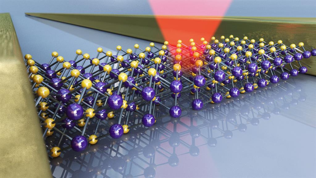
Artistic sketch of a polarized laser exciting surface currents in the topological insulator Bi2Se3, which is contacted by two gold electrodes. (c) nature.com and Cristoph Hohmann (NIM).
Original publication: C. Kastl, C. Karnetzky, H. Karl, A.W. Holleitner "Ultrafast helicity control of surface currents in topological insulators with near-unity fidelity" Nature Comm. 6, 6617 (2015).
02 Dec 2014
Graphene layer reads optical information from nanodiamonds electronically
In a recent publication in Nature Nanotechnology, we demonstrate that the spin of nitrogen-vacancy centers in diamond can be electronically read-out using a graphene layer on a picosecond time-scale. Nitrogen-vacancy centers in diamonds could be used to construct vital components for quantum computers. But hitherto it has been impossible to read optically written information from such systems electronically. The work was led by the group of Alexander Holleitner in collaboration with Frank Koppens (ICFO, Barcelona).

Image: Christoph Hohmann / NIM Link to press release Original publication: A. Brenneis, L. Gaudreau, M. Seifert, H. Karl, M.S. Brandt, H. Huebl, J.A. Garrido, F.H.L. Koppens, and A.W. Holleitner "Ultrafast electronic read-out of diamond NV centres coupled to graphene" Nature Nanotechnology 10, 135 (2015).
22 Nov 2014
Nanoday at the Deutsches Museum !
„Nano – what does that mean exactly? How is it able to work on that tiny scale? What is the use of the research results?" You will get answers to these and many other questions at first hand by our scientists. At the information booths you can do a lot of nano-experiments yourself and in the stage program professors will explain their cutting edge research projects. The program is completed by the comedian Georg Eggers who presents science with a twinkle in his eye. This year on Saturday 22nd November 10:00-17:00 you will have the chance to experience the world of nanoscience by visiting the NanoDay 2014 at the Deutsches Museum in Munich - Entrance to the exhibit is entirely free ! click here for more information!
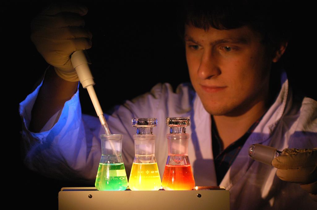
11 Oct 2014
Tag der offenen Tür am Walter Schottky Institut (WSI) und Zentrum für Nanotechnologie und Nanomaterialien (ZNN)
Programm des Walter Schottky Instituts: Programm Das komplette Programm gibt es hier: forschung-garching.de
05 Sep 2014
New research group on diamond quantum sensors
A newly established Emmy-Noether research group has joined the WSI on the 1st of September 2014. Its research will focus on quantum sensors based on color centers in diamond and their application in life science, in particular nuclear magnetic resonance (NMR) spectroscopy of single biomolecules.The new group is led by Friedemann Reinhard, formerly a senior scientist in the lab of Prof. Dr. Jörg Wrachtrup at the University of Stuttgart. He has been at the forefront of research on diamond quantum sensors for several years, demonstrating among other results the first detection of NMR signals from a 5nm small sample volume.
Friedemann and his group will join department E24 (Prof. Jonathan Finley). Funding for the group is provided by the Emmy-Noether program of the Deutsche Forschungsgesellgeschaft (DFG), a support program providing outstanding young scientists with an independent research group. All of us at the Walter Schottky Institut wish the new group a highly successful start and look forward to fruitful collaborations over the coming years !
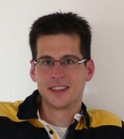
17 Jul 2014
The art of photon "bundling"...
In a recent publication in Nature Photonics led by WSI alumnus Fabrice Laussy in collaboration with Jonathan Finley's group, we published a paper in which a quantum optical light source can emit optical energy strictly via "bundles" of curious N-photon quanta, where N can be any integer. Remarkably, what appears to be the simplest possible configuration in cavity quantum electrodynamics - a single-mode optical cavity containing a two-level system like a quantum dot - is capable of exhibiting a broad range of interesting, and even counter-intuitive behaviours when pumped with an external laser. Fabrice has written an excellent article on the art of photon buldling on his blog.
02 Jul 2014
Hocheffiziente nichtlineare Metamaterialien für die Laser-Technik
Trotz aller Fortschritte gibt es noch immer nicht für alle gewünschten Frequenzen geeignete Laser-Systeme. Manche dieser Frequenzen kann man mit Frequenzverdopplern erzeugen, die nichtlineare optische Eigenschaften nutzen. Wissenschaftler der Technischen Universität München (TUM) und der University of Texas (Austin, USA) haben nun einen optischen Baustein entwickelt, dessen nur 400 Nanometer dicke Schicht, 100-mal dünner als ein menschliches Haar, verschiedenste Frequenzen verdoppeln kann und eine Million mal effizienter ist als traditionelle Materialien mit nichtlinearen optischen Eigenschaften.Weiter zur TUM Pressemeldung...
11 Mar 2014
IBM Ph.D. Fellowship for Bernhard Loitsch
Bernhard Loitsch, Ph.D student at the Walter Schottky Institut, has received the prestigious IBM Ph.D Fellowship award. This award is an intensely competitive worldwide program, which recognizes the great potential of individual Ph.D. students in their very early career as well as the quality of the research institution in focus areas of interest to IBM. Dr. Heike Riel, IBM Fellow and Manager of the Nanoscale Electronics group at IBM Research – Zurich, will act as his mentor throughout this fellowship. The award aims to strengthen collaborations between IBM and the core research group of the awardee at WSI-TUM. It covers a $20.000 stipend for one academic year and can be renewed yearly. Bernhard Loitsch is a Ph.D. student supervised by Dr. Gregor Koblmüller and Prof. Jonathan Finley in the Quantum Nanomaterials Group of E24. He investigates the epitaxial growth of GaAs-based nanowire heterostructures as well as their optical and electrical properties.
22 Jan 2014
Official opening of E24 optics laboratories in the Walter Schottky Institut after renovation works!
Recently, it was our great pleasure to welcome Dr. U. Kirste from the Bayerische Staatsministerium für Wissenschaft, Forschung und Kunst (Bavarian Science Ministry) during a visit to the group E24 of the Walter Schottky Institut. It was a great opportunity for Prof. Finley and colleagues to discuss current and future research activities. Moreover, after many months in which the first group of laboratories were renovated and prepared for new experiments, we could officially declare the optical laboratories "open" and drink a toast to our future successes ! The hard work building up the laser spectroscopy experiments has now begun, students and staff working tirelessly over the Christmas vacations - check back later in spring 2014 to see how we are getting along!
|

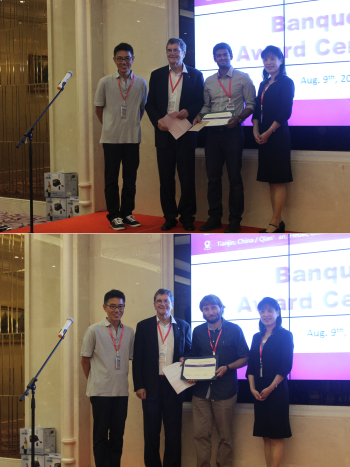
 Walter Schottky Institut