|
Photonics & Optoelectronics
|
|
"Photonic and optoelectronic phenomena on the nanometer scale are at the heart of fundamental science and technology. The institute explores various optoelectronic systems, ranging from quantum emitters, plasmonic nano-structures, embedded semiconducting tunneling barriers, to ultrafast THz circuits for future information technologies."
|
|
Current Work
|
|
 |
|
|
|
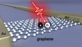
Optoelectronic phenomena on the nanometer scale include thermo-electric and photovoltaic processes. Atom-scale interfaces, local heat distributions, contact morphologies, and the dielectric environments are key parameters to optimize such nano-devices.
Finley
Holleitner
Stutzmann
Wurstbauer
|
|
|
 |
|
|
|
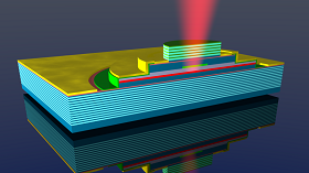
Vertical Cavity Surface Emitting Laser diodes (VCSELs) are nanoscale semiconductor lasers with light emission perpendicular to the chip surface. With their low power consumption, on-wafer testing-capability, easy fiber coupling and packaging, longitudinal single-mode emission, and suitability for 2D-array integration they are highly attractive for numerous applications in communications and sensing.
Belkin
|
|
|
 |
|
|
|
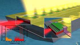
Quantum cascade lasers (QCLs) are based on intersubband transitions in quantum well (QW) structures. Differing from classical semiconductor lasers their emission wavelength can be tuned widely over the Mid- to Far-IR spectral range by the QW geometry and composition. They also possess a giant non-linear optical response which can be monolithically integrated into dual-wavelength QCLs to make efficient nonlinear devices extending the spectral coverage into the Near-IR (2-4µm) and Far-IR (15-200 µm) by sum- and difference-frequency generation, respectively.
Belkin
|
|
|
 |
|
|
|
Ultrafast processes in nanoscale materials range from femtosecond photoemission processes to charge, spin, and phonon relaxation dynamics, and the ballistic transport of charge carriers. We explore the time-scales and interplay of the various non-equilibrium dynamics in nanoscale circuits to drive on-chip THz circuits.
Finley
Holleitner
Kaniber
|
|
|
 |
|
|
|
The generation of electromagnetic fields at the nanoscale lie at the heart of a range of modern technologies ranging from photon-based information processing to light-harvesting for energy applications. We explore methods to concentrate optical fields to extreme lengthscales using plasmonics and photonic crystals and, thereby, control light-matter interactions over nanometer lengthscales.
Finley
Holleitner
Kaniber
Koblmüller
|
|
|
 |
|
|
|
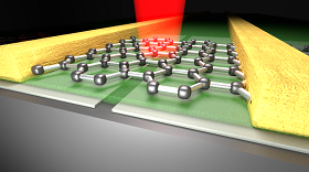
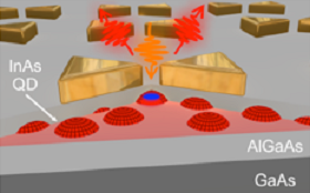
The monolithic integration of optically active materials onto silicon is key to the development of optical interconnects for chip-based data communications. We explore the growth of optically active group III-arsenide nanowire heterostructures on silicon and study their fundamental ultrafast optical and electro-thermal properties in order to test their viability as on-chip sources of coherent light.
Finley
Kaniber
Koblmüller
|
|
|
 |
|
|
|
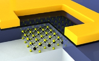
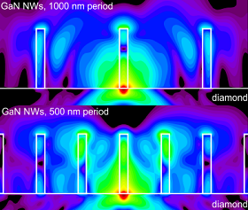
Nanowires made of GaN are transparent in the entire visible spectral region and can be doped n- or p-type to achieve a high electrical conductivity at the same time. Thus, GaN nanowires can be employed as versatile nano-antennas or nano-contacts in optoelectronics and photochemistry. By tuning the length, diameter, and spatial pattern of nanowires with the help of selective area epitaxy, it is possible to couple light efficiently in and out of NV-center qubits in diamond and, at the same time, tune the charge state of the center by applying a local electric field.
Finley
Sharp
Stutzmann
|
|
|
|

 Walter Schottky Institut