|
Nanofabrication
|
|
"We aim at structuring materials down to the atomic level or to dimensions specific to the envisioned experiment."
|
|
Current Work
|
|
 |
|
|
|
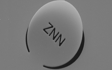
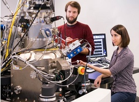
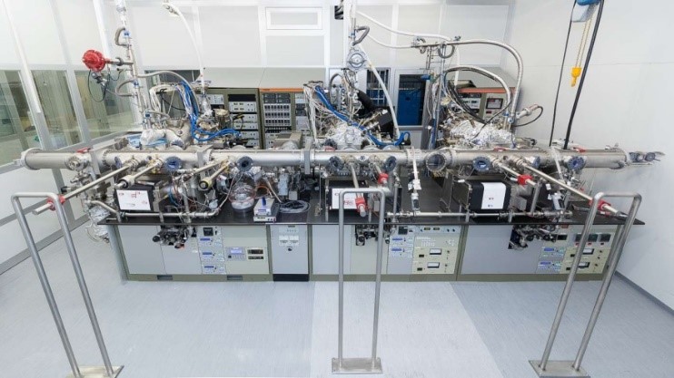
The Walter Schottky institute of the TUM operates the Center for Nanotechnologies and Nanomaterials (ZNN), as a shared nanofabrication facility. Students, researchers, and scholars from the greater scientific Munich area have access to state-of-the-art nanolithography and -analytic instruments for building and characterizing nanoscale electronic, optoelectronic, and photonic circuits. The nanofabrication methodologies include ebeam-, focused-ion-beam-, and helium-ion-lithography.
|
|
|
 |
|
|
|
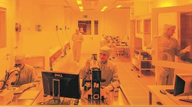
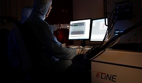
To keep the investigated nanoscale materials and circuits clean from micron-sized particles, all of us need to wear specific gowns in the clean room. The so-called ‘optical lithography’ utilizes light in the ultraviolet such that the clean room needs to be lightened in yellow. Our cleanroom is in general certified as class 4 and in some areas class 0.
|
|
|
 |
|
|
|
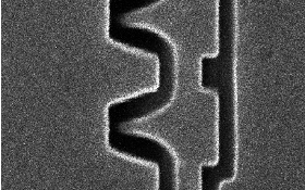
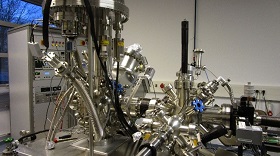
The helium ion microscope (HIM) allows structuring nanoscale materials on a lengthscale of sub-10 nm or even down to the single defect level. The HIM-lithography particularly works for atomistically thin materials, such as 2D materials, and semiconductor nanowires.
|
|
|
 |
|
|
|
The focused ion beam (FIB) lithography typically utilizes Ga+-ions to locally sputter materials such as metals into nanoscale circuits. Moreover, we take the FIB to fabricate thin lamellas of solids as investigated in transmission electron microscopy.
|
|
|
 |
|
|
|
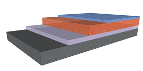
Atomic layer deposition (ALD) is a thin-film deposition technique based on the sequential use of a gas phase chemical process. We use the technique to fabricate thin dielectric and metallic layers for instance for catalytic systems.
|
|
|
 |
|
|
|
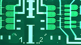
The optical lithography is our work horse for defining circuits on a sub-micron structure size but with macroscopic extensions. The optical lithography allows depositing complex circuits made from thin metal layers on top of various substrates.
|
|
|
 |
|
|
|
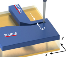
The atomic force microscope (AFM) allows characterizing the surface of nanoscale materials with a resolution close to the atomic limit. We further use our AFM to structure thin materials into local circuits with source and drain contacts by a 'ploughing technique'.
|
|
|
 |
|
|
|
The ultraviolet and x-ray photoelectron spectroscopy (UPS & XPS) rely on the photoemission of electrons from thin surface layers and allow characterizing their elemental composition. We analyze nanoscale materials promising for energy conversion applications.
|
|
|
 |
|
|
|
The electron beam-lithography is the standard method to define plasmonic structures down to the few nanometer scale.
|
|
|
 |
|
|
|
... including a wide range of III-V seminconductors (group III Arsenides, Phosphides, Antimonides, Nitrides) and atomically thin nanomaterials (graphene and transition metal dichalcogenides).
|
|
|
|

 Walter Schottky Institut