The Walter Schottky Institut (WSI) is a central institute of Technische Universität München (TUM) that was founded in order to strengthen the interaction between basic physics and semiconductor electronics research. The idea to create such an interdisciplinary research facility first emerged in the early 1980’s. Semiconductor heterostructures had become a very popular field of research at that time following the discoveries of many novel electronic and optical effects in low dimensional systems such as two-dimensional electron gases and quantum wells. The most prominent discoveries in semiconductor physics were the Quantum Hall Effect by Klaus von Klitzing in 1980 (Nobel prize 1985) and the Fractional Quantum Hall Effect by Daniel Tsui, Horst Störmer and Arthur Gossard in 1982 (Nobel prize for Tsui, Störmer and Laughlin (theory) in 1998). At the same time various technologically relevant novel electronic and optical devices were proposed and developed. Specific examples include Quantum Well Lasers (Henry, Dingle, Holonyak, Tsang and others), Resonant Tunnelling Diodes (Esaki, Tsu, Chang and others), or High Electron Mobility Transistors (Abstreiter, Ploog, Mimura and others). These devices provided new functionality and led to a wide variety of applications for example in the field of communication technology (satellite receivers, optical communication, cellular phones). The achievements were based on the excellent materials control through epitaxial techniques, especially molecular beam epitaxy. These modern materials technologies allowed control of layered structures on an atomic scale and were widely employed in industrial laboratories in United States and Japan as basis for the realization of novel devices. In Munich, this kind of research and development was embedded in a collaborative research center funded by the German Research Association (SFB 128 “Elementare Anregungen an Oberflächen”), where in one research area two-dimensional electron systems at semiconductor interfaces were studied. This work was concentrated at the chair of Fred Koch at the Physics Department of TUM and the project leaders in the early eighties were Fred Koch, Klaus von Klitzing and Gerhard Abstreiter. Around the same time closer interactions developed between the TUM physics groups and the research and development center of Siemens AG in the area of microstructured devices. In addition, a joint research program funded by Volkswagenstiftung was established between Gerhard Abstreiter and Klaus von Klitzing of E16 with Erich Gornik’s group at the University of Innsbruck. The successful projects were strongly dependent on high quality materials which were provided by only a very few sources; namely Günter Weimann from the research laboratory of Deutsche Bundespost in Darmstadt and Klaus Ploog from Max-Planck-Institut Stuttgart. At the time, these two laboratories were the only groups in Germany which could grow high quality GaAs based heterostructures. There was a strong need for an interdisciplinary research environment that combined high quality semiconductor hetero- and nanomaterials technology with basic physics as well as device development.
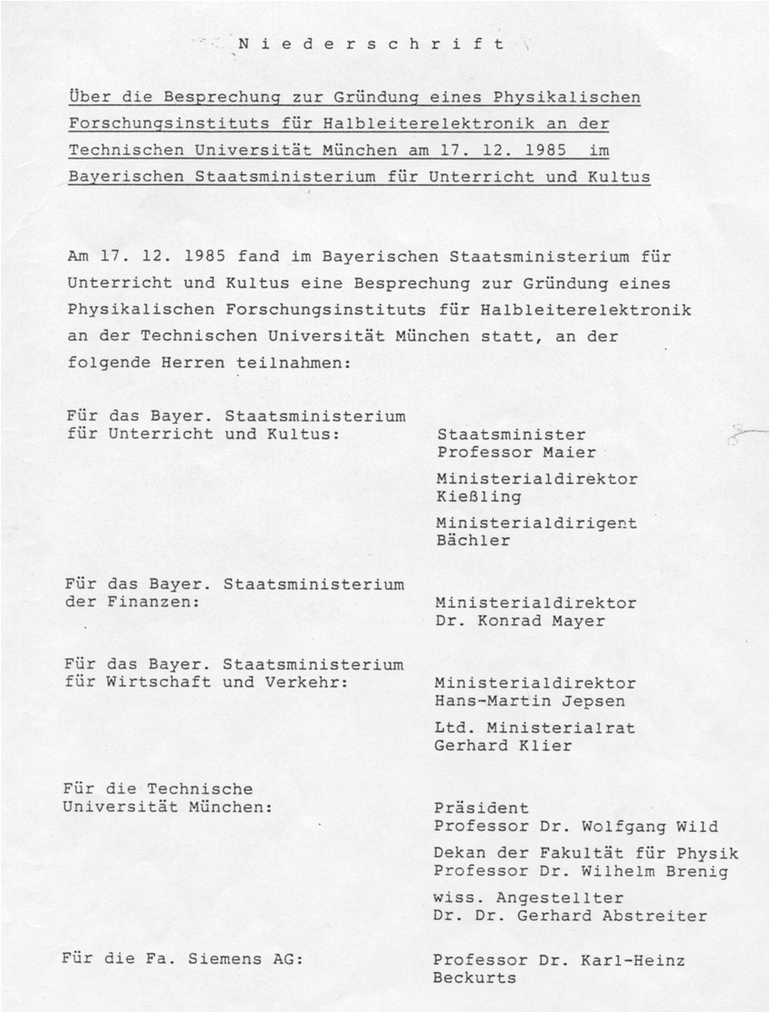
Fig. 1: Meeting to discuss the establishment of a institute for semiconductor and microelectronic research.
In February 1985, Gerhard Abstreiter wrote a memorandum with the suggestion to create a new institute with a specific focus on semiconductor micromaterials research and device development. This proposal was discussed with Karl-Heinz Beckurts, who at that time was head of the Siemens research laboratories and had already expressed strong interest in strengthening collaborations between industry and the TUM. In September 1985 the proposal received additional impetus after it was announced that Klaus von Klitzing would receive the Nobel Prize in Physics for his discovery of the Quantum Hall Effect. Klaus von Klitzing had just left the Physics Department of TUM in early 1985 to take up a directorship at Max-Planck-Institut für Festkörperforschung in Stuttgart. The Nobel Prize had an extremely positive impact on the initiative for the realization of a new research facility at TUM and both Fred Koch and Wilhelm Brenig, at that time dean of the physics department of TUM, wrote supporting letters in October / November 2005 suggesting the creation of a research institute focusing on semiconductor physics and electronics. The name “Walter Schottky Institut” was suggested by Karl-Heinz Beckurts in a meeting at the Physics Department in Garching. Walter Schottky was a famous and well known physicist who worked for Siemens from 1927 until 1976 when he died close to his 90th birthday. His research combined basic physics with development of novel devices. The combination of materials technology, fundamental physics and device applications was planned to become the central mission and principle goal of the new institute. The idea to create such a research facility was strongly supported by Klaus von Klitzing and Wolfgang Wild, president of TUM and later Bavarian Minister for Science, Research and Art.
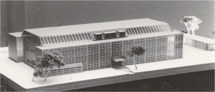
Fig. 2: A vision becomes reality – architects model the Walter Schottky Institute.
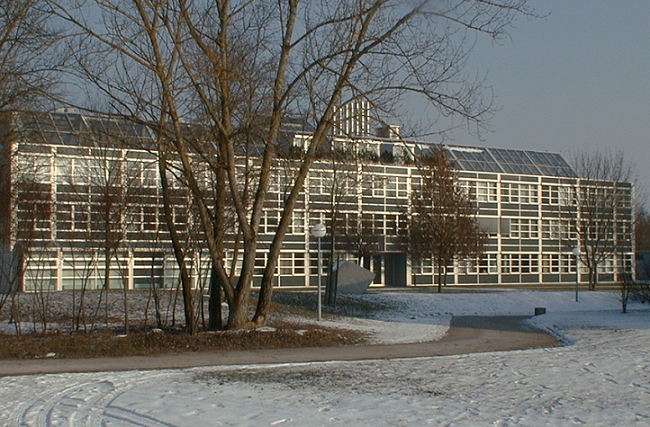
Already on December 17, 1985, there was a meeting at the Bayerische Staatsministerium für Unterricht und Kultus with Bavarian State Minister Hans Maier to discuss the boundary conditions for the foundation of a research institute for semiconductor electronics at TUM in collaboration with Siemens AG (figure 1). Following an additional meeting of Klaus von Klitzing with Bavarian’s Minister President Franz Josef Strauß in February 1986 the final decision to create such an interdisciplinary research institute was made. It was the year of the hundredth birthday of Walter Schottky. From then on it took only about two years until the new laboratories became operational in 1988 (figure 2).
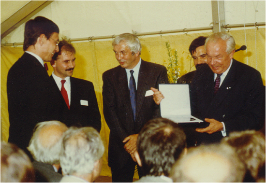
Fig. 3: Inauguration ceremony on July 14th, 1988.
Research in the new institute started in May, a few months before the official inauguration and opening ceremony on July 14th, 1988 (figure 3). This exceptionally short time for planning and construction of a modern institute building was made possible by the excellent cooperation between the Siemens AG, the Bavarian ministries and the TUM. Interests of university, industry and politics met here in a rare but fortunate circumstance. The realization of the WSI was based on an official TUM-Siemens collaboration effort called “Sonderforschungseinheit mikrostrukturierte Bauelemente”. As discussed already in the foreword, it was the first example where industry took the responsibility for the construction of a laboratory building at TUM. Many people were particularly helpful in setting up the new research institute: The strong commitment of Karl-Heinz Beckurts was essential for the whole project. In the early planning stage he became victim of a terrible bomb attack by terrorists belonging to the Rote Armee Fraktion (RAF) where he and his chauffeur were murdered. It is extremely sad and regrettable that he was no longer amongst us at the official opening of the WSI in summer 1988 (figure 3).

 The Walter Schottky Institut (WSI) is a central institute of Technische Universität München (TUM) that was founded in order to strengthen the interaction between basic physics and semiconductor electronics research. The idea to create such an interdisciplinary research facility first emerged in the early 1980’s. Semiconductor heterostructures had become a very popular field of research at that time following the discoveries of many novel electronic and optical effects in low dimensional systems such as two-dimensional electron gases and quantum wells. The most prominent discoveries in semiconductor physics were the Quantum Hall Effect by Klaus von Klitzing in 1980 (Nobel prize 1985) and the Fractional Quantum Hall Effect by Daniel Tsui, Horst Störmer and Arthur Gossard in 1982 (Nobel prize for Tsui, Störmer and Laughlin (theory) in 1998). At the same time various technologically relevant novel electronic and optical devices were proposed and developed. Specific examples include Quantum Well Lasers (Henry, Dingle, Holonyak, Tsang and others), Resonant Tunnelling Diodes (Esaki, Tsu, Chang and others), or High Electron Mobility Transistors (Abstreiter, Ploog, Mimura and others). These devices provided new functionality and led to a wide variety of applications for example in the field of communication technology (satellite receivers, optical communication, cellular phones). The achievements were based on the excellent materials control through epitaxial techniques, especially molecular beam epitaxy. These modern materials technologies allowed control of layered structures on an atomic scale and were widely employed in industrial laboratories in United States and Japan as basis for the realization of novel devices. In Munich, this kind of research and development was embedded in a collaborative research center funded by the German Research Association (SFB 128 “Elementare Anregungen an Oberflächen”), where in one research area two-dimensional electron systems at semiconductor interfaces were studied. This work was concentrated at the chair of Fred Koch at the Physics Department of TUM and the project leaders in the early eighties were Fred Koch, Klaus von Klitzing and Gerhard Abstreiter. Around the same time closer interactions developed between the TUM physics groups and the research and development center of Siemens AG in the area of microstructured devices. In addition, a joint research program funded by Volkswagenstiftung was established between Gerhard Abstreiter and Klaus von Klitzing of E16 with Erich Gornik’s group at the University of Innsbruck. The successful projects were strongly dependent on high quality materials which were provided by only a very few sources; namely Günter Weimann from the research laboratory of Deutsche Bundespost in Darmstadt and Klaus Ploog from Max-Planck-Institut Stuttgart. At the time, these two laboratories were the only groups in Germany which could grow high quality GaAs based heterostructures. There was a strong need for an interdisciplinary research environment that combined high quality semiconductor hetero- and nanomaterials technology with basic physics as well as device development.
 Walter Schottky Institut