|
Engineered Nanomaterials
|
|
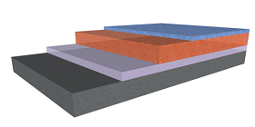
"The growth of materials with highly controlled composition, well-defined crystal structure, low-defect and dislocation density and ultra-high purity is a cornerstone of research into opto-electronics, photonics, quantum technologies and energy sciences. In WSI, we operate state-of-the-art growth systems for the preparation of III-V semiconductors like group-III arsenides, phosphides and nitrides, MBE for transition metal dichalcogenides, CVD for 2D-materials and thin-film deposition systems."
|
|
Current Work
|
|
 |
|
|
|
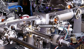
We place strong emphasis on the in-house ability to grow ultra-high purity materials and heterostructures using UHV molecular beam epitaxy and vapor phase methods. Hereby, various groups are working on the growth of novel In(Ga,Al)As–based quantum dots and nanowires on silicon, group-III phosphides for long wavelength VCSELs for telecommunications and gas sensing, (In,Ga,Al)N-based heterostructures for optoelectronic and thermoelectric applications and, most recently, atomically thin 2D-semiconductors.
Belkin
Finley
Koblmüller
Sharp
Stutzmann
|
|
|
 |
|
|
|
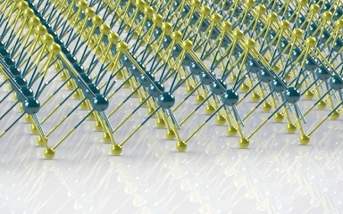
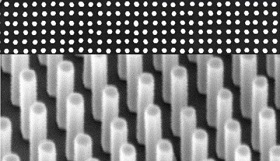
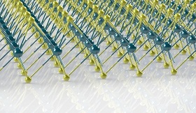
Semiconductor Nanowires (NWs) will play a key role for next generation electronic, photonic, sensor and energy device applications. These one-dimensional nanostructures offer new functionalities due to their unique surface-to-volume ratio, reduced density of states and modified charge carrier dynamics. This allows additional control of electronic, optical and thermal properties not feasible in conventional planar thin film technology. Unlike planar heterostructures, the materials that can be combined is much broader, allowing e.g. highly luminescent III-V materials to be grown in a NW geometry on silicon substrates.
Finley
Koblmüller
Stutzmann
|
|
|
 |
|
|
|
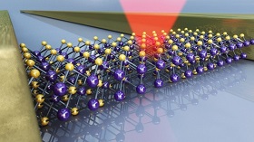
Two-dimensional (2D) materials are particularly suited for optoelectronic experiments. The materials are atomically thin and some of them, such as monolayer MoS2, exhibit a direct band gap in the visual spectral range. 2D materials can be laterally structured to functional circuits down to few nanometers, a scale fundamentally limited only by the materials’ Bohr radius. We investigate the non-equilibrium charge, valley, and spin properties in the materials ranging from single exciton to many-body phenomena.
Brandt
Finley
Holleitner
Kaniber
Koblmüller
Müller
Sharp
Wurstbauer
|
|
|
 |
|
|
|
Atomic layer deposition (ALD) has emerged as a powerful method to precisely synthesize conformal thin films, even over high aspect ratio nano- and meso-structures. Self-limiting surface reactions and low deposition temperatures allow fabrication of novel interfaces and materials that are not accessible by other methods. In our work, we create and study the properties of ALD generated heterojunctions, functional interfaces, and disorder-controlled catalysts.
Sharp
Stutzmann
|
|
|
 |
|
|
|
Topological materials are quantum materials where the electron and spin properties are dominated by topology. Particularly, three-dimensional topological insulators are a class of Dirac materials with two-dimensional metallic surface states featuring spin-momentum locking, i.e., each momentum vector is associated with a spin locked perpendicularly to it in the surface plane. We implement such materials as thin as only a few atomic layers into nanoscale circuits.
Holleitner
|
|
|
 |
|
|
|
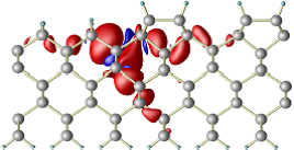
Defects critically determine the behavior of electronic materials and devices. We develop highly sensitive techniques to study defects based on combinations of electron spin resonance and transport measurements (electrically detected magnetic resonance), allowing us to observe as few as 50 defects and to understand their dynamics.
Brandt
Finley
Holleitner
Kaniber
Reinhard
Stutzmann
Wurstbauer
|
|
|
|

 Walter Schottky Institut