As worldwide energy demand increases, conventional energy resources, such as fossil fuels , will be exhausted in the not-too distant future. Therefore, the development and use of alternative energy resources, especially our only long-term natural resource, the sun, is essential. The solar cells is considered a major candidate for obtaining energy from the sun, since it can convert sunlight directly to electricity with high conversion efficiency, can provide nearly permanent power at low operating cost and is virtually free of pollution.The solar cell was first developed by Chapin, Fuller, and Pearson in 1954 using a p-n silicon junction with an efficiency of 6 %. To date, solar cells have been made in many other semiconductors, using various device configurations and employing single crystal, poly-crystal, and amorphous thin-film structures. The efficiencies have been improved continuously over the last 50 years with world records ranging between 24 % for a single crystalline silicon solar cell and 36 % for tandem structures. Major world wide research activities are: 1) The development of new semiconductors which will absorb most of the solar radiation within micrometers. To achieve this goal semiconductors with direct optical band gaps are required. 2) Effective light trapping structures are needed to improve the absorption of light in established thin film solar cells. 3) To improve the efficiency of thin film silicon based solar cells micro- or mono-crystalline layers are required. The development of new deposition techniques which allow the growth of mono crystalline thin film semiconductors on substrates like glass and metal sheets is therefore a major issue.
In our group we focus on the following targets:
SiGe alloys
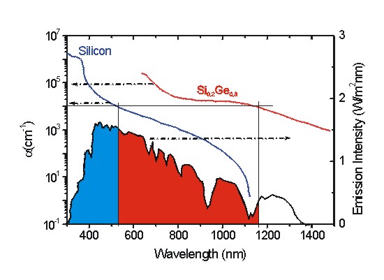
Currently, we explore the growth of Si0.2Ge0.8 alloys. This semiconductor has a direct optical band gap at 1.4 eV. Most of the radiated energy of the sun will be absorbed by such an solar cell within 1 micrometer (see Fig. 1). We evaporate amorphous SiGe mixtures on glass by use of a ultra high vacuum system and apply pulsed laser induced crystallization.
Fig. 1: The optical absorptions of one micrometer thick silicon and SiGe with respect to the sun emission.
Research activities are:
Optimization of the SiGe mixture with respect to optical and electronic properties
Growth of large grain or mono crystalline layers on glass.
Realization of p-n junctions to explore the solar cell parameters.
Light trapping structures
By proper design of thin film solar cells with appropriate light trapping structures refection and transmission losses can be minimized. Amorphous and polycrystalline thin film silicon solar cells are therefore grown on statistically rough substrates like Asahi TCO. These substrates are however too expensive to be used for mass production.
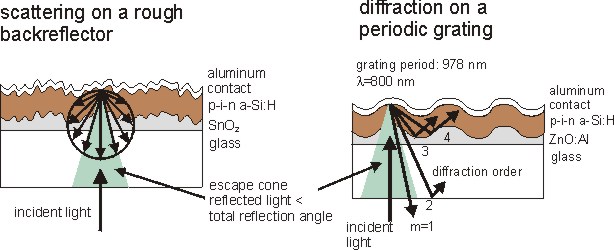
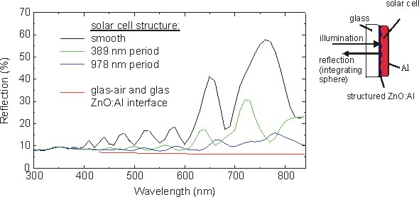
As an alternative we realized periodic light trapping structures in silicon or TCO with periods in the micrometer regime (see Fig. 2). We apply a laser interference technique which is fast, can be applied to large areas and cheap. Instead of light scattering we use diffraction effects to guide the light into the thin absorber layers. Reflectivity losses are reduced significantly by these structures (see Fig. 3). In addition, enhance built-in electric fields are expected which should improve the solar cell efficiency.
Fig. 2: A comparison of light trapping structures. On the left statistical rough substrates are used and overgrown. On the right side our periodically structured substrate is used to optimize light trapping.
Fig. 3: Comparison of refection losses of thin film solar cells deposited on different substrates. The periodically structured solar cell (p = 978 nm) shows minimized reflection losses.
Research activities are:
Application of periodic light trapping structures into thin film I) a-Si:H/a-SiGe:H or ii) a-Si:H/mc-Si tandem solar cells.
Characterization of the optical and electronic solar cell parameters.
Large grain silicon
The growth of large grain silicon on substrates like glass or metal sheets is achieved by pulsed laser crystallization. For details see page laser processing!
Funding
Bundesministerium für Forschung und Technologie under: 0329814A


 Walter Schottky Institut