Material processing with lasers takes advantage of all the characteristics of laser light. The high energy density and directionality achieved with lasers permits strong localized heat- or photo-treatment of materials with spatial resolution below one micrometer. The pulsed and monochromatic light allows the control of depth of heat treatment or selective excitation. The laser beam can be moved to process large areas, is a sterile tool and is no subject to wear and tear.
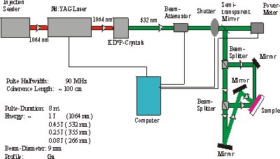
Fig. 1: Nd:YAG-Laser system
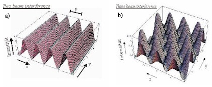
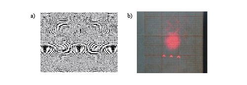
In our group we use a Nd:YAG laser system as shown in Fig 1. The laser beam intensity profile is Gaussian. We process semiconductors using the primary beam ("homogeneous laser processing"), apply interferenc effects to generate periodic intensity profiles as shown in Fig. 2a,b or use digital holograms shown in Fig. 3a,b.
Fig. 2 a) Intensity pattern generated by two interfering beams b) Intensity pattern generated by interference of three beams
Fig. 3 a) Digital Hologram and b) the Intensity pattern generated by the hologram shown in Fig. 3a.
Some examples of laser processed semiconductors
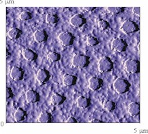
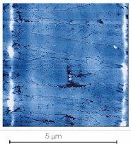
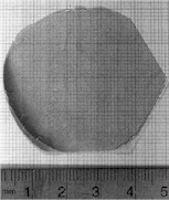
Laser processing is applied to manufacture laterally structured electrodes (Fig. 4) for solar cells which improve the built-in electric field of thin film solar cells and give rise to light trapping. An other application is the photo chemical processing of DFB gratings for InP and GaN laser (Fig. 5). Large grain silicon for photovoltaic and display applications is grown on glass as shown in Fig. 6 by the scanning interference laser crystallization. Laser beam induced lift-off of GaN from sapphire substrates is applied to generate free standing thin film GaN substrates, LEDs or other electronic devices (see Fig. 7).
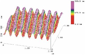
Fig. 4: Periodic structured microcrystalline Si electrode for thin film solar cells
Fig. 5: GaN DFB structure generated by photo chemical laser processing. The period is 240 nm.
Fig. 6: Scanning interference laser crystallized silicon on glass. Large Si grains are grown which extend several microns in scanning direction and about 1 micron perpendicular to it.
Fig. 7: Free standing GaN of about 100 micrometer Thickness. It has been lifted from the sapphire substrate by pulsed laser illumination


 Walter Schottky Institut