|
Semiconductor Quantum Nanomaterials - Research
Group leader: PD Dr. Gregor Koblmueller (Chair of Prof. Dr. Jonathan Finley)
Our research activities on semiconductor quantum nanomaterials aim at four different domains. These encompass "Advanced Synthesis" using ultrahigh-purity molecular beam epitaxy methods, "Functional Properties" to interrogate key structure-property-function relationships, "Integrated Photonics" describing the development of novel on-chip integrated nanolasers and quantum light sources, and "Quantum Electronics" addressing new concepts in nanowire-based quantum transport, in topological semi-/ superconductors, and nano-thermoelectrics research.
ADVANCED SYNTHESIS
![[research]](../subgroups/Koblmueller/Koblmueller21.jpg)
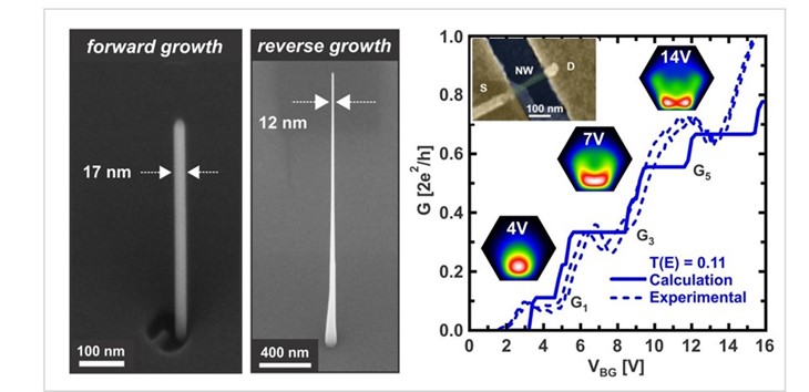
A major workhorse for our research on advanced nano-systems/devices are innovative semiconductor nano- & quantum-heterostructures created by design using accurately controlled synthesis methods. Specifically we employ ultrahigh-purity molecular beam epitaxy (MBE) dedicated to III-V compound semiconductors (arsenides / antimonides), group-III nitrides as well as new classes of emerging 2D materials. The latter are synthesized in a new MBE-cluster system in collaboration with the MWM sub-group. Currently, a substantial effort in synthesis is on III-V nanowires (NW), which offer unique capabilities in heterostructure and crystal phase engineering, as well as site-selective growth and deterministic incorporation of atomically engineered low-dimensional quantum systems. The following selection of key publications gives a brief view into ongoing activities in growth/synthesis research of 1D-NWs and their quantum heterostructures.
Personnel
M. Bissolo, C. Doganlar, H. Esmaielpour, B. Haubmann, G. Hirpessa, H. W. Jeong, S. Meder, T. Schreitmüller, A. Uhle
Recent publications

|
| H. W. Jeong, et al., “Sb-mediated tuning of growth and exciton dynamics in entirely catalyst-free GaAsSb nanowires”, Small 19, 2207531 (2023). |
|  |
| F. Del Giudice, et al., “Epitaxial type-I and type-II InAs-AlAsSb core-shell nanowires on silicon”, Appl. Phys. Lett. 119, 193102 (2021).
|
|  |
| D. Ruhstorfer, et al., “Growth dynamics and compositional structure in periodic InAsSb nanowire arrays on Si (111) grown by selective area molecular beam epitaxy", Nanotechnology 32, 135604 (2021). |
| 
|
| B.
Sun, et al., “Dislocation-induced thermal transport anisotropy in
single-crystal group-III nitride films”, Nature Materials 18, 136
(2019). |
| |
|
|
|
FUNCTIONAL PROPERTIES
![[research]](../subgroups/Koblmueller/Koblmueller25.jpg)
To establish the as-grown quantum nano-structures for various different devices, understanding of their structure-function-property relationships is indispensable to predict their performance. This requires advanced high-resolution spectroscopy and imaging methods to resolve properties quantitatively and at the nanoscale. Here, we employ a whole toolbox of different nano-metrology techniques to link specific structural and morphological features with electrical, optical, mechanical and thermal properties. Examples of such methods include electrical scanning probe microscopy (SPM) techniques, high-resolution electron and ion-beam microscopy, µRaman spectroscopy, time- and spatially resolved µPL spectroscopy (vis-to-midIR), absorption spectroscopy, etc. Typical examples of research in this field are illustrated in various selected publications.
Personnel
M. Bissolo, C. Doganlar, H. Esmaielpour, B. Haubmann, G. Hirpessa, H. W. Jeong, S. Meder, T. Schreitmüller, A. Uhle
Recent publications
|
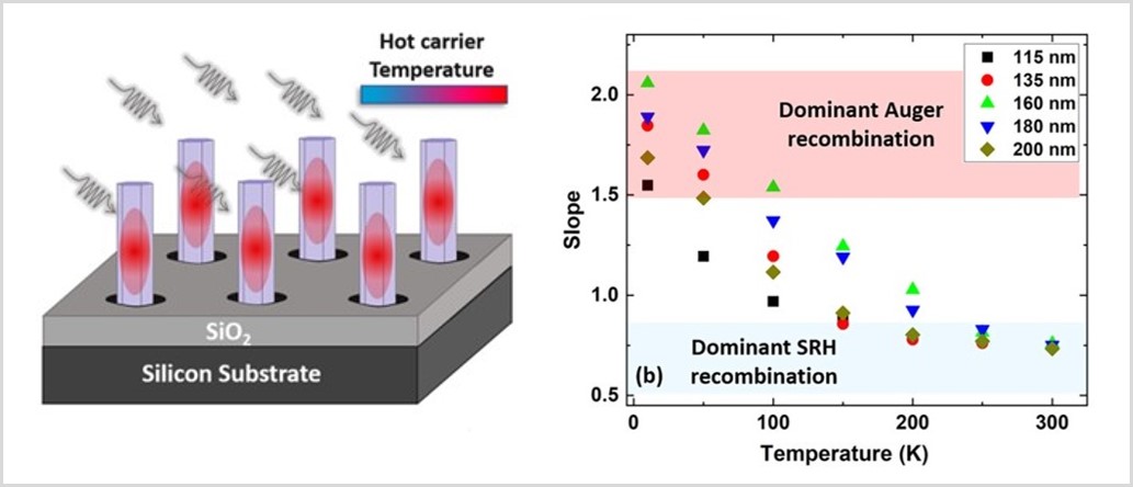
| H. Esmaielpour, et al., "Influence of Auger heating and Shockley-Read-Hall recombination on hot carrier effects in InGaAs nanowires", Phys. Rev. B 109, 235303 (2024).
|
|  |
| D. Sandner, et al., "Hot electron dynamics in InAs-AlAsSb core-shell nanowires" ACS Appl. Energy Mater. 6, 10467 (2023).
|
|  |
| M. O. Hill, et al., "3D Bragg coherent diffraction imaging of extended nanowires: Defect formation in highly strained InGaAs quantum wells", ACS Nano 16, 20281 (2022).
|
|  |
| D. Ruhstorfer, et al., "Demonstration of n-type behavior in catalyst-free Si-doped GaAs nanowires grown by molecular beam epitaxy", Appl. Phys. Lett. 116, 052101 (2020).
|
|
INTEGRATED PHOTONICS
![[research]](../subgroups/Koblmueller/Koblmueller29.jpg)
One of our current research directions is to develop high-performance integrated photonic, quantum photonic and optoelectronic devices based on on-chip monolithically integrated quantum nanowire (NW) heterostructures. Specific examples include NW-based lasers and non-classical single photon emitters based on NW-QD (-quantum dot) devices for next-generation information technology, quantum communication and sensing. Hereby, an important task is to explore the optical and photonic responses of the respective systems using advanced confocal luminescence spectroscopy along with simulations, where e.g. the effects of the quantized electronic structure, light-matter interactions, or the coupling of light to on-chip photonic circuits are probed. The following key publications illustrate our current work on integrated photonic NW-based devices and their properties.
Personnel
B. Alparslan, C. Doganlar, B. Haubmann, N. Isaev, H. W. Jeong, S. Meder, T. Schreitmüller, S. Werner, J. Zöllner
Recent publications
|
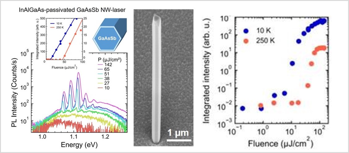
| P. Schmiedeke, et al., "Low-threshold single ternary GaAsSb nanowire lasers emitting at silicon transparent wavelengths", Appl. Phys. Lett. 124, 071112 (2024).
|
|  |
| H. W. Jeong, et al., "Axial growth characteristics of optically active InGaAs nanowire heterostructures for integrated nanophotonic devices", ACS Appl. Nano Mater. 7, 3032 (2024).
|
|  |
| N. Mukhundhan, et al., "Purcell enhanced coupling of nanowire quantum emitters to silicon photonic waveguides", Optics Express 29, 43068 (2021).
|
|  |
| P. Schmiedeke, et al., "Low-threshold strain-compensated InGaAs/(In,Al)GaAs multi-quantum well nanowire lasers emitting near 1.3 µm at room temperature", Appl. Phys. Lett. 118, 221103 (2021).
|
|
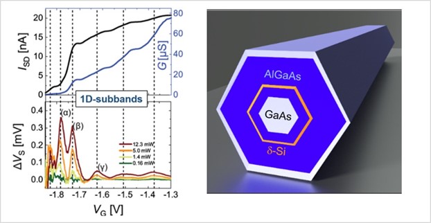
QUANTUM ELECTRONICS
![[research]](../subgroups/Koblmueller/Koblmueller33.jpg)
The materials under investigation are also prime candidates for advanced quantum transport studies and future electronic devices with performance perspectives that go well beyond those of classical field-effect transistors. A major focus of our work aims therefore at developing high-mobility III-V based NW channels as well as systems with large spin-orbit interaction (e.g. InAs NW) for topological superconductor-semiconductor hybrids. Important goals here are to understand and optimize the semi-classical & quantum transport phenomena in dependence of channel & device design, quantum confinement, structural properties, etc. using low-noise, temperature- and field-dependent transport spectroscopy. In addition, we also explore new concepts in quantum-thermoelectrics and hot-carrier solar cells via energy-selective NW-contacts in these systems. Recent highlights are summarized in the respective selection of key publications.
Personnel
N. S. Aydin, H. Esmaielpour, G. Hirpessa, S. Meder, T. Schreitmüller, J. Solomon
Recent publications 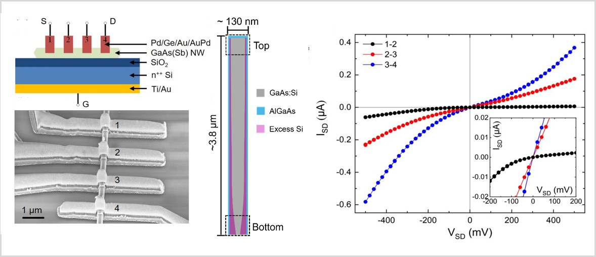
|
| T. Schreitmüller, et al., "Spatial dependence of dopant incorporation and electrical transport in Si-doped GaAs(Sb) nanowires", Phys. Rev. Mater. (2024).
|
| 
|
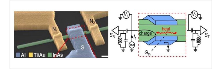
| A. O. Denisov, et al., "Charge-neutral nonlocal response in superconductor-InAs nanowire hybrid devices", Semicond. Sci. Technol. 36, 09LT04 (2021).
|
| 
|
| S. Fust, et al., "Quantum-confinement enhanced thermoelectric properties in modulation-doped GaAs-AlGaAs core-shell nanowires", Advanced Materials 32, 1905458 (2020).
|
| 
|
| F. del Giudice, et al., "Ultrathin catalyst-free InAs nanowires on silicon with distinct 1D subband transport properties", Nanoscale 12, 21857 (2020). |
|
|
|


![[research]](../subgroups/Koblmueller/Koblmueller17.png)
![[research]](../subgroups/Koblmueller/Koblmueller18.png)
![[research]](../subgroups/Koblmueller/Koblmueller19.jpg)
![[research]](../subgroups/Koblmueller/Koblmueller20.png)
 Walter Schottky Institut