|
Quantum Sensing and Spectroscopy of Low Dimensional Materials (QS) - Research
Group leader: Andreas Stier
2D materials
Two-dimensional
materials such as transition-metal dichalcogenides are atomically thin
crystalline materials with interesting optical properties. 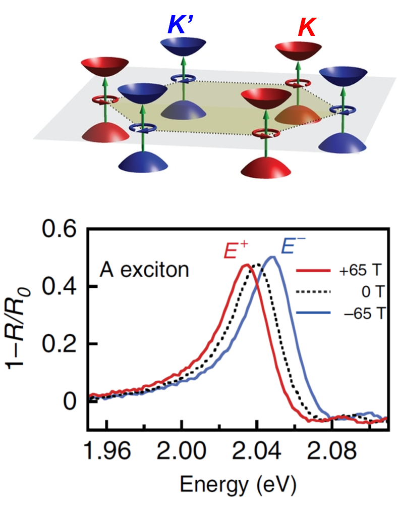
For example, the
optical properties of 2D transition-metal dichalcogenides (TMDs) such as MoSe2
or WS2, are dominated by excitons, Coulomb-bound particles comprised
of an electron and a hole. Because 2D materials are so thin, any material
directly adjacent to the TMD layer affects the properties of those excitons. We
are interested in the following questions:
-
What are the fundamental properties
of TMDs?
-
How does the dielectric / magnetic
/ topological environment of an atomically thin TMD affect the excitons?
-
Can we engineer the environment of
TMDs in such a way as to enable interesting physical phases or to create
interesting devices?
Present collaborators:
Richard Schmidt (MPQ), Christopher Gies, Matthias
Florian, Alexander Steinhoff (U. Bremen). Relevant
publications:
1.
“Magnetooptics of exciton Rydberg states
in a monolayer semiconductor”
Phys. Rev. Lett. 120, 057405
(2018), Editors Choice.
2.
”Probing the influence of dielectric
environment on excitons in monolayer WSe2: Insight from high
magnetic fields”
Nano Lett. 16, 7054 (2016)
3.
“Exciton diamagnetic shift and valley
Zeeman splitting in monolayer WS2 and MoS2 to 65 Tesla”
Nature Comm. 7, 10643 (2016) 4. "Controlling exciton many-body states by the electric field effect in monolayer MoS2"
Phys Rev. Research 3, L022009 (2021)
Quantum Sensing of 2D materials
In conventional
spectroscopy, the state of a system is measured by investigating either the energy
eigenstates or
the excitations out of the ground state. Using these pathways, we can attempt to understand the intricacies of
emergent quantum phases.
However, especially in 2D systems, interactions are strongly enhanced and may
become so complicated that more information is needed in order to form a
complete picture. This is especially true for novel magnetic 2D materials, where spin, charge and valley degrees of freedom as well
as spontaneously
broken symmetries at interfaces can come into play.
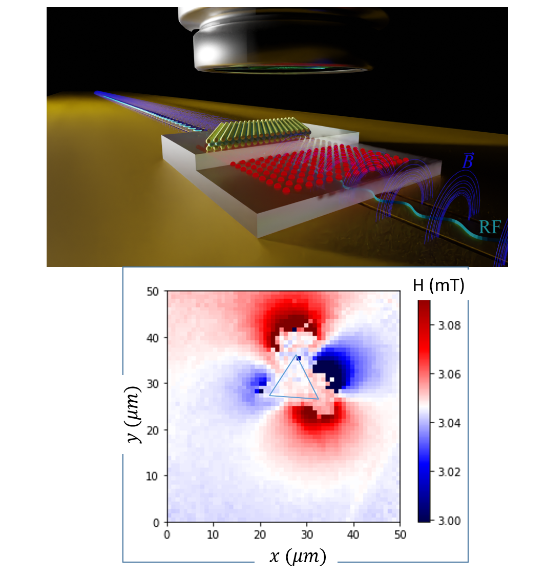
We are
utilizing nitrogen vacancy centers in diamond for imaging of magnetic phases of
novel 2D heterostructures. These highly sensitive sensors are essentially a
quantum 2-level system that is influenced by the electric or magnetic fields of
a proximized 2D material. Thus we can quantitatively image the quantum state of
a specimen. Present collaborators: Dominik Bucher (TUM), Zdenek Sofer (UCT Prague), Jaroslav Fabian (U. Regensburg).
Localized excitons in 2D
materials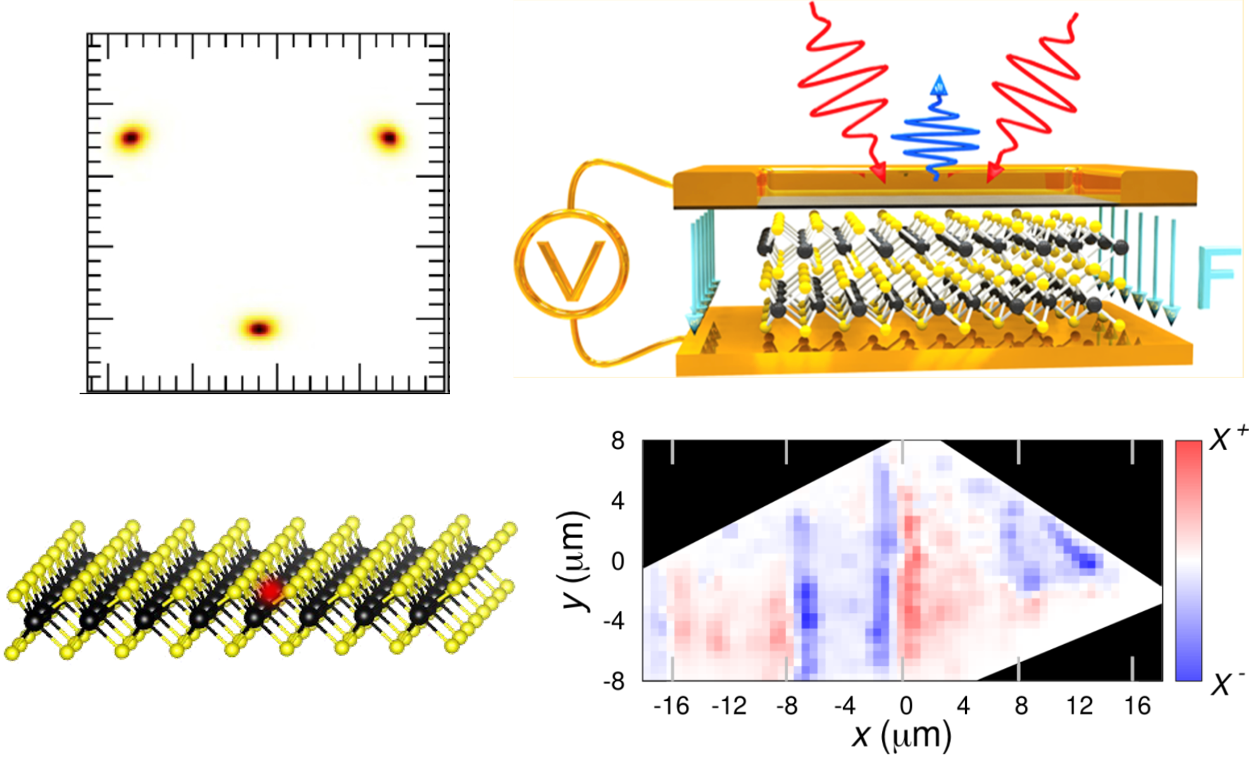
Localized excitons
in 2D materials have shown to be sources for
single photon emission. We follow
two avenues for excitons localization in order to create single photon sources
for quantum light applications exciton localization through dielectric engineering
and strain-induced exciton localization. Our goal is to couple light from such
localized emitters into photonic structures.
Present
collaborators: Christopher Gies (U. Bremen)
Katia Gallo (U. Stockholm)
Fei Ding (U. Hannover)
R. Haug (U. Hannover)
This work is supported by the DFG through the SPP 2244.
Relevant publications: 1. “Charged exciton kinetics in monolayer MoSe2 near ferroelectric domain walls in periodically poled lithium niobate"
Nano Letters 21, 959 (2021)
2D perovskites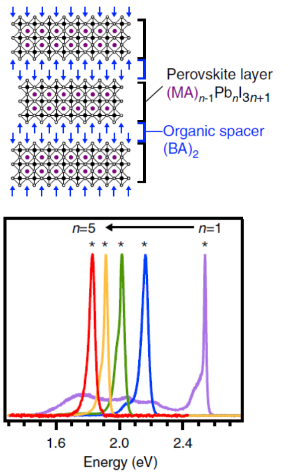
Similar to
conventional III-V semiconductor superlattices, Ruddlesden-Popper halide
perovskites are quantum well structures formed by two-dimensional layers of
halide perovskites semiconductors, separated by bulky organic spacer layers.
This layered structure can be tuned by varying the perovskite layer thickness and
the composition of the organic layer.
Although efficient
opto-electronic devices were made from such materials, fundamental questions
concerning the nature of optical resonances remain. We strive to understand the
basic optical properties of these fascinating materials.
Collaborators: J.C. Blancon (Rice University)
Relevant
publications:
1.
“Scaling law for excitons in 2D perovskite
quantum wells”
Nature Comm. 9, 2254 (2018) 2. "Managanese doping for enhanced magnetic brightening and circular polarization control of dark excitons in parametric layered hybrid metal-halide perovskites"
Nature Comm. 12, 1 (2021)
|


 Walter Schottky Institut