Surface functionalization of wide-gap semiconductors
The use of semiconductor devices as biochemical sensors requires their funtionalization e.g. with proteins, which allow specific molecules or chemical processes to be monitored selectively. For stability reasons, these functionalization layers are best attached covalently. Several methods are available to chemically bind molecules to semiconductor surfaces. Depending on the initial termination of the surface by H or OH groups, one generally uses either the so-called hydrosilylation or the silanization routes. In recent years, we have systematically investigated the hydrosilylation of single-crystalline Si, amorphous hydrogenated Si, Si nanowires and Si nanocrystals.
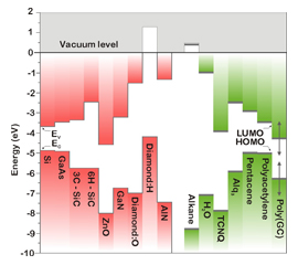
Alkyl layers formed via hydrosilylation on Si substrates show a very good electrical insulation as well as low defect densities of at the interface. However, if charge transport is desired across the functionalization, alkyl layers on Si are less than optimal. One reason can be seen directly from the diagram: The large offset between the conduction and valence bands of Silicon and the corresponding highest occupied and lowest unoccupied molecular orbitals of the molecules in the functionalization layer (HOMO and LUMO, respectively) impedes charge transport. One way to decrease this offset is to use semiconductors such as diamond, group-III nitrides or SiC with a large band gap. We are studying different routes for the covalent attachment of alkyls on these substrates and characterize the resulting heterostructures with respect to their structural, electronic and vibrational properties, with a special emphasis on SiC.
Selected publications
Functionalization of 6H-SiC surfaces with organosilanes
Applied Physics Letters 92 153301 (2008)
S. J. Schoell, M. Hoeb, I. D. Sharp, W. Steins, M. Eickhoff, M. Stutzmann, M. S. Brandt
Direct biofunctionalization of semiconductors: A survey
Feature article, physica status solidi a 203 3424 (2006)
M. Stutzmann, J. A. Garrido, M. Eickhoff, M. S. Brandt


 Walter Schottky Institut