|
Welcome to the Brandt group
Group leader: Prof. Dr. Martin Brandt
Doping in Silicon nanocrystals
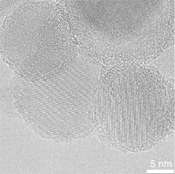
Traditionally, semiconductors are structured laterally with the help of lithography. In particular for large-area electronic devices such as displays and RFID tags, it would be interesting to develop fabrication methods based on printing, which requires inks containing semiconductor particles. To date, such inks usually contain organic semiconductors or precursors for the formation of semiconducting polymers. However, using plasma deposition techniques, Si nanocrystals can be produced in large quantities which can then be dispersed in a variety of liquids to form inorganic inks. We are actively studying the application of these Si-based inks to the fabrication of thin films and devices. In particular, we currently investigate the efficiency of the doping of these nanocrystals with B or P and the laser-induced sintering of thin films formed from Si nanocrystal inks. One very promising application could be devices for thermoelectric power conversion, where a suitable tailoring of the nanocrystal thin films could lead to a low thermal conductivity while keeping the electrical conductivity high.
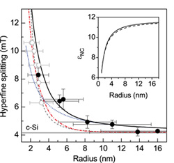
A fundamental physical aspect of nanocrystals of special interest to the Brandt group is the doping of Si nanoparticles. The overall doping efficiency can be estimated with the help of mass spectrometry in combination with optical and electrical measurements. However, using electron spin resonance, we can learn further details about the microscopic structure of donors in nanocrystals. As an example, the figure shows the increase of the localization of the Phosphorus donor wavefunction in nanoparticles when the nanocrystal radius is reduced. This data is obtained from the observation of the hyperfine interaction between the donor spin and the nuclear magnetic moment of the 31P nucleus. Detailed modeling shows that at low diameters quantum confinement due to the abrupt change in the potential at the nanocrystals governs the localization, while at larger diameters changes in the dielectric constant of the nanoparticles lead to localization.
Selected publications
-
Electronic properties of doped silicon nanocrystal films
Journal of Applied Physics, in print (2008)
R. Lechner, A. Stegner, R. Pereira, R. Dietmueller, M. S. Brandt, A. Ebbers, M. Trocha, H. Wiggers, M. Stutzmann
-
Electronic transport in phosphorus-doped silicon nanocrystal networks
Physical Review Letters 100 026803 (2008)
A. R. Stegner, R. N. Pereira, K. Klein, R. Lechner, R. Dietmueller, M. S. Brandt, M. Stutzmann, H. Wiggers
-
Thermoelectric effect in laser annealed printed nanocrystalline silicon layers
physica status solidi-rapid research letters 1 262 (2007)
R. Lechner, H. Wiggers, A. Ebbers, J. Steiger, M. S. Brandt, M. Stutzmann
Collaborations
Funding
- EU (PSYNANO)
- DFG (Nos. SFB 631, GK 1240)
- Evonik Degussa S2B Nanotronics
- State of North Rhine-Westfalia
|
|
|


 Walter Schottky Institut