RESEARCH
Head of Group: Prof. Dr. Alexander Holleitner
Our research projects focus on the following main directions:
Single-atom circuits
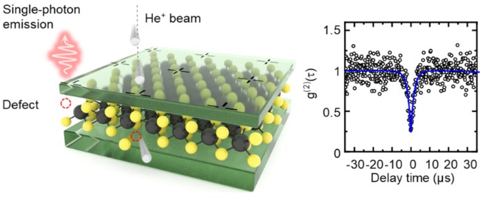
We recently demonstrated how to generate optically active defects in atomically thin 2D materials on a spatial scale of below 10 nm,
such that scalable opto/electronics based on individual atomic states seems at reach. Until now, this goal was reserved only to
materials and methods in the ultra-high vacuum. We use a helium-ion microscope (HIM) to generate individual defects, e.g. in
semiconducting MoS
2. Our single-defect technology is principally applicable to the wide range of 2D materials with more than
a thousand different materials and is compatible with standard cleanroom manufacturing steps. This combination makes it possible
to realize first devices based on single defects, such as gate-switchable single photon emitters and photodetectors or even solar
cells based on individual atomic defects. At the same time, fundamental processes, such as the coherent single electron tunneling
dynamics and many-body interactions of localized states in a Fermion boson mixture are experimentally accessible.
Present collaboration partners: Jonathan Finley (TUM), Frank Jahnke (Bremen), Kai Müller (TUM), Alex Weber-Bargioni (Berkeley).
BACK-TO-TOP
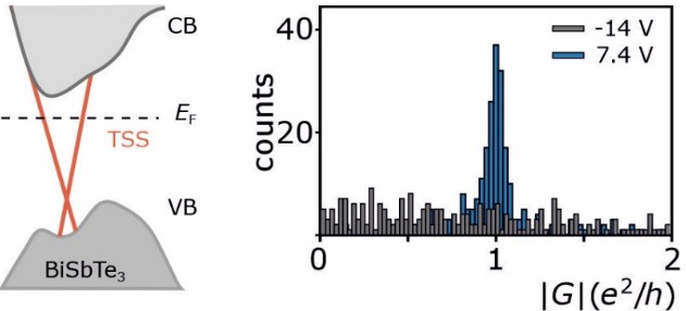
Topological materials and electronics
Topological surface states are very promising for future opto/electronic circuits, since computing schemes can be envisaged
where the information carrying surface state is protected by topology. Van der Waals materials and their heterostructure are
an ideal platform to engineer and explore topological states. On the one hand, we can control and break the relevant symmetries
of the Hamiltonian at will by interfacing different van der Waals materials with different symmetries. On the other hand, we
can directly address the symmetry of the electron-Bloch states in the van der Waals crystal by external electric field in atomic
field effect structures. In turn, a wide range of non-trivial, i.e. topological quantum phenomena can be explored, such as the
orbital Edelstein effect, Berry plasmons or even the interplay of plasmons and fringe states in quantum spin Hall-systems.
Monolayers of Weyl semi-metals, such as WTe
2, also have a superconducting phase far from charge neutrality. As a result,
exotic phenomena such as Higgs and Majorana modes seem to be possible in the near future in such topological atomistic
materials and field-effect heterostructures.
Present collaboration partners: Marko Burghard (MPI Stuttgart), Yongqing Li (IOP Bejing).
BACK-TO-TOP
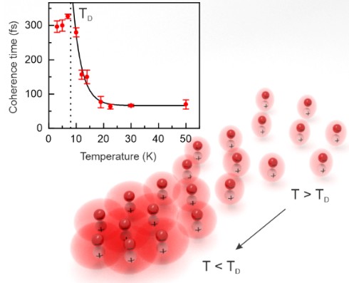
Excitonic Many-Body States including Bose-Einstein Condensates
Increasing the interaction strength between quasi-particles in solid-state materials can cause strong correlations,
collective phenomena and the transition to large-scale quantum phases, for example to a Bose-Einstein condensate.
Heterostructures made of semiconducting 2D materials, such as MoSe
2 and WSe
2, are ideal systems to realize a condensation of
excitons. The latter are Coulomb-bound electron hole pairs. The heterostructures enable large exciton binding energies, long
photoluminescence lifetimes, as well as a permanent exciton dipole, which allows the manipulation of the exciton ensembles,
e.g. via electric fields. In one of our current studies, we observe several signatures regarding photoluminescence intensity,
linewidth, temporal coherence and excitonic propagation dynamics in accordance with the predicted condensation temperature
of an excitonic Bose-Einstein condensation at about 10 Kelvin. This allows us to investigate quantum mechanical many-body
physics in nano-structured circuits. In particular, the Berezinskii-Kosterlitz-Thouless transition to a superfluidic
excitonic phase at very low temperatures (<1 K) and also the Mott transition to a degenerate electron-hole-fermi gas at
high excitonic densities appear experimentally accessible. With our advanced nanolithography, e.g. using HIM, we design such
coherent multi-particle circuits and investigate them for nanophotonic applications.
Present collaboration partners: Ursula Wurstbauer (University of Münster), Andreas Knorr (TU Berlin).
BACK-TO-TOP
Towards femtosecond on-chip electronics
The vision of this research topic is to generate electric current pulses with a duration of only a few femtoseconds
for an on-chip signal conversion at the interface between electronics and optics, the so-called THz-gap. For signal
generation we use amongst others, photo-emission processes, such as multiphoton absorption and strong field tunnel
processes in plasmonic nanocontacts; but also femtosecond processes within solid state materials. The signal
propagation occurs via electromagnetic THz modes in coplanar strip conductors. For the on-chip THz-detection, we are
working on an electrical detection on the 100 fs scale and faster. Currently we reach 350 fs by using the relaxation
dynamics in amorphous silicon photo-switches. Our group manufactures all circuits in our own laboratory, and
we use phase-stable femtosecond lasers to drive the on-chip THz circuits coherently. Intriguingly, atomically thin
2D materials can be integrated into the THz circuits without much effort, such that the 2D materials can act as
functional THz modulators. In the same way, the electron and heat dynamics in the 2D materials can be investigated
on a femto- to picosecond timescale.
Present collaboration partner: Reinhard Kienberger (TUM).
BACK-TO-TOP
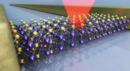
Nanofabrication
We are heading the Center for Nanotechnologies and Nanomaterials (ZNN), which is a shared nanofabrication facility
of the Walter Schottky Institute of TUM. Students, researchers, and scholars from the greater scientific Munich area
have access to state-of-the-art nanolithography and nanoanalytic instruments for building nanoscale electronic,
optoelectronic, and photonic circuits. The methodologies include electron beam-, focused-ion-beam-,
and helium-ion-beam lithography.
BACK-TO-TOP
Open positions
We are always looking for highly motivated students. Interested applicants should contact Prof. Holleitner for an
informal discussion on the opportunities available.
Acknowledgement
For all above research directions, we thank the European Research Council (ERC), the International Graduate School
for Science and Engineering of TUM (IGSSE), the
Bavaria California Technology Center (BaCaTec) and the Deutsche
Forschungsgemeinschaft (DFG) for funding in several projects. In particular, we are grateful for the support of
the excellence clusters
Munich Center for Quantum Science
& Technology (MCQST) and
e-conversion.
BACK-TO-TOP


 Walter Schottky Institut