Our research projects are focused on developing compact room-temperature optoelectronic and integrated photonics
devices and systems operating in the mid-infrared (mid-IR, λ ≈ 2.5-30 µm) and terahertz (THz, λ ≈ 30-300 µm) spectral range.
We also exploit opportunities offered by the new mid-IR and THz photonics technologies for applications. Selected current
research projects in the group are listed below.
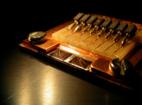
(Left) A laser bar with several THz DFG-QCLs on a copper heatsink.
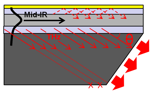
(Right) Schematic of a Cherenkov THz DFG-QCL. The active region (light grey) is designed to
provide both mid-IR gain and giant nonlinearity for THz DFG. THz radiation is emitting into
the substrate in the so-called Cherenkov phase-matching scheme.
THz spectral range is teeming with mainstream concepts. However, it is still in need of a convenient and compact semiconductor
source and detector technology. In particular, THz radiation sources are bulky, complex in operation, and expensive to manufacture.
Real-world applications require room-temperature broadly-tunable or frequency-comb THz sources that are similar in operation
simplicity and mass producibility to diode lasers and mid-IR quantum cascade lasers (QCLs).
We have recently achieved significant progress in the development of such sources [1,2]. Our devices are based on
efficient frequency mixing inside of dual-wavelength mid-IR QCLs. Their active regions are quantum-engineered to
provide a giant nonlinearity for difference-frequency generation (DFG) with population inversion [1,2] and their
waveguides are designed for Cherenkov phase-matching of DFG that enables THz extraction through the substrate [3].
As a result, these devices (referred to as THz DFG-QCLs) can now provide up to nearly 2 mW of peak THz power output
and over 10 µW of continuous-wave THz power at room temperature [1,2]. A schematic of a Cherenkov THz DFG-QLC is
shown in the figure on the right. Show more
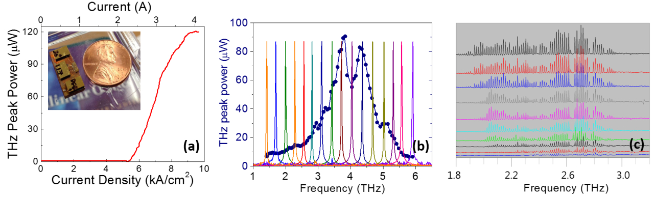
A typical single mode device performance is shown in Fig. 1(a). We have also demonstrated that THz DFG-QCL chips
can be continuously tuned over nearly the entire 1-6 THz range using an external cavity setup [3-5] or in monolithic
configurations [6,7], see Fig. 2(b). We have further recently confirmed that, in continuous-wave operation, these devices
provide a narrow (sub-MHz) emission linewidth which makes them suitable to be used as local oscillators for heterodyne
spectroscopy [8]. The THz DFG-QCL platform holds a high promise for developing efficient broadband THz frequency
comb sources for spectroscopic and metrological applications.
Our ongoing work is aimed at improving the THz radiation outcouping efficiency (estimated to be below ~5% in the current
devices) [9,10], enhancing the optical nonlinearity in the QCL active regions to increase THz output power, improving
device thermal packaging, generating THz frequency combs, developing miniature broadly-tunable THz systems, and
demonstrating compact semiconductor-based THz instrumentation such as spectroscopy and imaging systems, dual-comb
spectrometers, and microscopy systems.
Fig. 1. (a) THz DFG-QCL laser bar (inset) and room-temperature light output vs current characteristic for a 1.7-mm-long
and 25-µm-wide ridge-waveguide THz DFG-QCL with single-mode emission at 4 THz. (b) Room-temperature emission spectra and
THz power output of the external cavity THz DFG-QCL system at different external cavity grating positions. (c) Multi-mode
THz emission spectra at different pump currents from a THz DFG-QCL device.
REFERENCES
K. Fujita, S. Jung, Y. Jiang, J.H. Kim, A Nakanishi, A. Ito, M. Hitaka, T. Edamura, and M.A. Belkin,
“Recent progress in terahertz difference-frequency quantum cascade laser sources,” Nanophoton.7, 1795-1817 (2018).
M.A. Belkin and F. Capasso, “New frontiers in quantum cascade lasers: high performance room temperature
terahertz sources,” Phys. Scr.90, 118002 (2015).
K. Vijayraghavan, Y. Jiang, M. Jang, A. Jiang, K. Choutagunta, A. Vizbaras, F. Demmerle, G. Boehm,
M. C. Amann, and M. A. Belkin, “Broadly tunable terahertz generation in mid-infrared quantum cascade lasers,”
Nature Commun.4, 2021 (2013).
Y. Jiang, K. Vijayraghavan, S. Jung, F. Demmerle, G. Boehm, M.-C. Amann, and M.A. Belkin “External
cavity terahertz quantum cascade laser sources based on intracavity frequency mixing with 1.2-5.9 THz tuning range,”
J. Opt.16, 094002 (2014).
Y. Jiang, K. Vijayraghavan, S. Jung, A. Jiang, J.H. Kim, F. Demmerle, G. Boehm, M.C. Amann, and M.A.
Belkin, “Spectroscopic study of terahertz generation in mid-infrared quantum cascade lasers,” Sci. Rep.6, 21169 (2016).
S. Jung, A. Jiang, Y. Jiang, K. Vijayraghavan, X. Wang, M. Troccoli, and M.A. Belkin, “Broadly tunable
monolithic room-temperature terahertz quantum cascade laser sources,” Nature Commun.5, 4267 (2014).
A. Jiang, S. Jung, Y. Jiang, K. Vijayraghavan, J. Kim, and M.A. Belkin, “Widely tunable terahertz source
based on intra-cavity frequency mixing in quantum cascade laser arrays,” Appl. Phys. Lett.106, 261107 (2015).
L. Consolino, S. Jung, A. Campa, M. De Regis, S. Pal, K. Fujita, A. Ito, M. Hitaka, S. Bartalini,
P. De Natale, M.A. Belkin, and M.S. Vitiello, “Spectral purity and tunability of terahertz quantum cascade laser
sources based on intra-cavity difference frequency generation,” Sci. Adv.3, e160331 (2017).
J.H. Kim, S. Jung, Y. Jiang, K. Fujita, M. Hitaka, A. Ito, T. Edamura, and M.A. Belkin “Double-metal
waveguide terahertz difference-frequency generation quantum cascade lasers with surface grating outcouplers,”
Appl. Phys. Lett.113, 161102 (2018).
S. Jung, J. Kim, Y. Jiang, K. Vijayraghavan, and M. A. Belkin, "Terahertz difference-frequency quantum
cascade laser sources on silicon," Optica 47, 38-43 (2017). Close
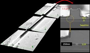
Mid-IR QCLs transfer-printed to silicon-on-sapphire.
Near-infrared (wavelengths approximately in the range of 1-2.5 microns) photonic integrated circuits (PICs) based on
the silicon-on-insulator (SOI) or III-V platforms have undergone a tremendous expansion in recent years, driven initially by
applications in fiber-optics communications and optical interconnects and later expanding to beam combining and steering,
chemical and biological sensing, and frequency comb generation. Near-infrared PIC systems are now commercialized for
several different applications by companies such as Infinera, Sisco Systems, SICOYA, and many others.
In contrast to the near-infrared spectral range, mid-IR laser-based systems have so far been designed around free-space
optics. Integration of a semiconductor laser with a suitable mid-IR photonics platform will enable the development of
mid-IR PICs for a wide range of applications from spectroscopy and sensing to beam steering aund ab nd new frequency
generation. We have recently started investigating approaches for developing mid-IR PICs using both silicon and
III-V platforms. Show more
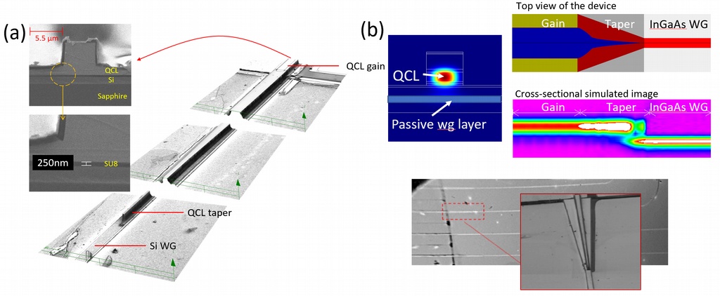
Figure 2(a) shows the electron microscope image of a mid-IR QCL epi-transferred to Silicon-on-Sapphire (SOS) wafers
using 250-nm-thick SU-8 epoxy as an adhesive. Efficient coupling of mid-IR light from the laser cavity to silicon
waveguides was achieved using tapered QCL waveguides as shown in Fig. 3(a) after Ref. [1]. Similar transfer-printing
methods can be used to integrate other mid-IR light sources, such as diode lasers and interband cascade lasers (ICLs)
with silicon waveguides.
Hybrid mid-IR systems based on III-V laser materials transferred to silicon photonic waveguides are expected to
perform well with mid-IR diode lasers and ICLs that have relatively low (few tens of milliwatts) optical powers
and thermal power dissipation. However, long-wavelength room-temperature operation of these devices is limited
to the 5-6 microns spectral range. In addition, the use of the Si-based platforms limits the spectral range of
mid-IR PICs to below 7 μm due to optical absorption in Si.
QCLs are currently the only room-temperature electrically pumped semiconductor light sources that can operate
in the entire mid-IR range (from 3 to 15 microns) with optical powers over 1 W. Given the very high thermal
dissipation in QCL active regions, achieving long-term reliability and continuous-wave operation of heterogeneously
integrated devices on silicon platforms is challenging. Therefore, we have recently started working on homogeneous
integration of mid-IR QCLs with low-loss III-V passive waveguides epitaxially grown on InP substrates, see Fig. 2(b).
The homogeneous integration approach uses materials, growth, and processing steps nearly identical to those used for
conventional high-performance mid-IR QCLs, which offers superior reliability and performance of photonic integrated circuits.
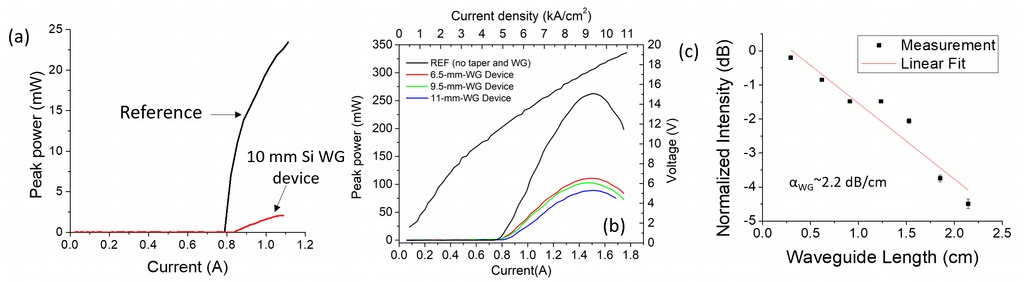
Devices integrated with III-V waveguides show more than an order of magnitude higher output power from passive waveguides,
compared to devices integrated with the SOS waveguides as shown in Fig. 3.
Ongoing and planned work include efforts to reduce the waveguide losses and the development of continuous-wave mid-IR
PICs for high-speed light modulation, beam steering, on-chip sensing, and nonlinear generation of new frequencies.
Fig. 2. (a) Scanning electron microscope image of a mid-IR QCL epi-transferred to Silicon-on-Sapphire (SOS) wafers
using 250-nm-thick SU-8 epoxy as adhesive. Also shown is the microscope image of the QCL waveguide taper that couples
light from the laser into the passive waveguide. (b) Schematic of the PIC based on homogeneous integration of
InGaAs/AlInAs QCLs with passive III-V waveguides. Shown is the cross-section of the laser/waveguide system, the
taper design, and the electron microscope image of processed devices.
Fig. 3. (a) Performance of a λ ≈ 4.6 µm QCL transfer-printed to SOS. Shown is the light output-current characteristic
of a reference edge-emitting device on SOS and a waveguide-coupled device [1]. (b) Similar results for monophonically
integrated QCLs on a III-V passive waveguiding platform [2]. (c) Optical losses in the fabricated III-V passive
waveguides at λ ≈ 4.6 µm [2].
REFERENCES
S. Jung, J. Kirch, J.H. Kim, L.J. Mawst, D. Botez, and M.A. Belkin, “Quantum cascade lasers transfer-printed on
silicon-on-sapphire,” Appl. Phys. Lett.111, 211102 (2017).
S. Jung, D. Palaferri, K. Zhang, F. Xie, Y. Okuno, C. Pinzone, K. Lascola, and M.A. Belkin, “Homogeneous photonic
integration of mid-infrared quantum cascade lasers with low-loss passive waveguides on InP platform,” Optica6,
1023-1030 (2019). Close
Nonlinear metasurface for second-harmonic generation.
The mid-IR and THz regions are particularly suitable for creating engineered materials based on the concepts of quantum-engineering
of electron states, plasmonics, and metamaterials. We have recently demonstrated the potential of this approach by creating large-area
ultrathin metasurfaces with record-high nonlinear optical response. The metasurfaces operate by coupling modes in
electromagnetically-engineered plasmonic nanoresonators with quantum-engineered intersubband nonlinearities in a thin semiconductor heterostructure.
Subwavelength thickness of our metasurfaces precludes phase matching constrains associated with traditional nonlinear optical
crystals and thus allows for broadband frequency conversion. Furthermore, since very low optical intensity is required to
produce strong nonlinear effects, our metasurfaces may be pumped using compact continuous-wave semiconductor lasers such
as QCLs or diode lasers. Continuously-pumped metasurfaces may be used, for example, to achieve self-referencing and frequency
shift of low-power microresonator-based optical frequency comb sources to anywhere in mid-IR and THz, to generate large amounts
of THz radiation using high-power mid-IR pump lasers (e.g., CO2 lasers or high-power QCLs), and to up-convert mid-IR and THz
optical signals for focal-plane-array imaging. Show more
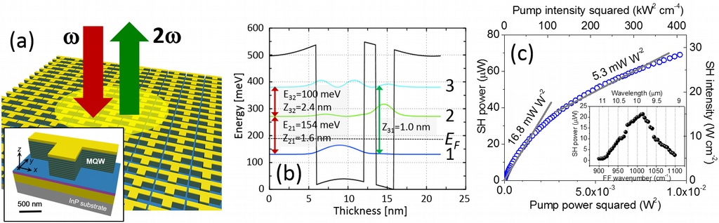
The basic schematic of the metasurface is given in Fig. 4 and its operation is explained in the figure caption.
We achieved over 0.075 % of mid-IR second-harmonic power conversion efficiency using only 15 kW/cm2 of pump intensity [1,2].
The second-order nonlinear susceptibility of our latest metasurfaces at low pump intensity is estimated to be over 106 pm/V,
4 orders of magnitude higher than that of traditional nonlinear materials such as LiNbO3. From the fundamental standpoint,
our metasurfaces provide the foundation for the “flat nonlinear optics paradigm” in which we can simultaneously produce
high nonlinear conversion efficiency and achieve full control of the wavefront of the nonlinear output, as demonstrated by us in Ref. [3].
We are now investigating numerous directions in which the effective nonlinearity and conversion efficiency of the
metasurfaces may be further improved, particularly, by optimizing plasmonic nanoresonator designs to achieve higher
field enhancement and higher nonlinear overlap integral [4,5] and by increasing the intersubband nonlinearity and
saturation intensity of the semiconductor heterostructure using more sophisticated MQW designs. Theoretical simulations
indicate that up to 10% of power conversion efficiency is possible in fully-optimized structures using input
intensities ~10-100 kW/cm2. Additional ongoing and planned future research on this topic include
Design and experimental testing of metasurfaces for THz difference-frequency generation [6];
Metasurfaces for efficient up-conversion of mid-IR and THz signals for detection and imaging;
Nonlinear metasurfaces for mid-IR and THz Raman lasing and other four-wave mixing processes such as phase conjugation and all-optical control;
Investigating quantum effects in individual highly-nonlinear nanoscale optical resonators [7].
Fig. 4. (a) Schematic of a representative nonlinear intersubband polaritonic metasurface metasurface. A thin (400-nm-thick)
layer of InGaAs/AlInAs multi-quantum well (MQW) heterostructure is used to produce the metal-MQW-metal nanocavities shown in the inset.
Gold is shown in yellow, titanium in blue, and platinum in magenta. Nanocavities are designed to have resonances at λ = 10 µm and 5 µm for
x- and y-polarized light, respectively. (b) A single period of the MQW structure designed for giant nonlinear susceptibility for second
harmonic (SH) generation at λ = 10 µm pump wavelength. (c) The SH output from the metasurface in (a) as a function of the λ = 10 µm pump
power (bottom axis) or intensity (top axis). Inset: SH power output as a function of the pump wavelength at the pump power of 35 mW.
REFERENCES
J. Lee, M. Tymchenko, C. Argyropoulos, P. Y. Chen, F. Lu, F. Demmerle, G. Boehm, M. C. Amann, A. Alu, and M.A. Belkin,
“Giant nonlinear response from plasmonic metasurfaces coupled to intersubband transitions,” Nature511, 65 (2014).
J. Lee, N. Nookala, J. S. Gomez-Diaz, M. Tymchenko, F. Demmerle, G. Boehm, M.-C. Amann, A. Alù, and M.A. Belkin
“Ultrathin second-harmonic metasurfaces with record-high nonlinear optical response,” Adv. Opt. Mat.4, 664-670 (2016).
N. Nookala, J. Lee, J.S. Gomez-Diaz, M. Tymchenko, F. Demmerle, G. Boehm, K. Lai, G. Shvets, M.-C. Amann, A. Alù,
and M.A. Belkin, “Ultrathin gradient nonlinear metasurface with a giant nonlinear response,” Optica3, 283-288 (2016).
N. Nookala, J. Xu, O. Wolf, S. March, R. Sarma, S. Bank, J. Klem, I. Brener, and M. A. Belkin,
“Mid-infrared second-harmonic generation in ultra-thin plasmonic metasurfaces without a full-metal backplane,” Appl. Phys. B.124, 132 (2018).
R. Sarma, D. de Ceglia, N. Nookala, M. Vincenti, S. Campione, O. Wolf, M. Scalora, M. Sinclair,
M. Belkin and I. Brener, "Broadband and efficient second-harmonic generation from a hybrid dielectric
metasurface/semiconductor quantum-well structure," ACS Photon.6, 1458 (2019).
M. Tokman, Z. Long, S. Al Mutairi, Y. Wang, V. Vdovin, M. Belkin, and A. Belyanin, “Purcell enhancement
of the parametric down-conversion in two-dimensional nonlinear materials,” APL Photonics4, 034403 (2019).
M. Tymchenko, J. S. Gomez-Diaz, J. Lee, M.A. Belkin, and A. Alù, “Highly-efficient THz generation using
nonlinear plasmonic metasurfaces,” J. Opt.19, 104001 (2017). Close
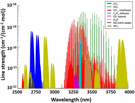
A portion of the mid-IR molecular fingerprint region with absorption lines of selected gases.
Gas sensing based on direct laser diode absorption spectroscopy is one of the most sensitive and
selective detection methods and it is widely used in industry. Because of their geometry, vertical
cavity surface emitting lasers (VCSELs) are known to have significant advantages over edge-emitting
diode lasers, including extreme compactness, about two orders of magnitude lower power consumption
(due to smaller active region volume), round (rather than elliptical) beam shape, and intrinsic
single-mode operation without the need for complex distributed feedback gratings used in single-mode
edge-emitting lasers (due to much smaller laser cavity size).
Mid-IR spectral range is often called the ‘molecular fingerprint region’ because any chemical compound can be
uniquely described by its molecular absorption fingerprint. The development of continuous-wave (CW) mid-IR
VCSELs is highly desired for the creation of compact chemical sensors with high detectivity and specificity.
Currently, however, such VCSELs do not exist. We are working on the development of CW room-temperature mid-IR
VCSELs in the wavelength range 3-5 µm. Show more
Due to current unavailability of CW VCSELs operating in the wavelength range of the fundamental molecular
roto-vibrational absorption lines, devices operating at shorter near-infrared (near-IR) wavelengths
(often around 1550 nm) are used to target the absorption lines corresponding to “overtones” (higher-order harmonics)
of fundamental molecular vibrations. However, these lines are typically about 2 orders of magnitude weaker
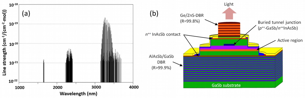
than the fundamental absorption lines. Figure 5(a) shows the absorption spectrum of methane displaying both
fundamental absorption lines around 3300 nm and overtone lines at 1550 nm and 2300 nm. Additionally, the
overtone line spectrum of molecular compounds is more complex and spectrally dense compared to the spectrum
of the fundamental lines. As a result, it is often difficult to select an overtone absorption line of a
target molecule that is free from interference produced by overtone lines of other gases.
Our research efforts focus on developing CW room-temperature mid-IR VCSELs operating in the 3-5 µm wavelength
range using InAlGaAsSb heterostructures grown on GaSb substrates. The schematic of a VCSEL structure is shown
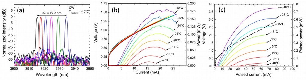
in Fig. 5(b). The Chair has produced devices that define the current state of the art in the mid-IR VCSEL
technology, including CW VCSELs at 3 µm wavelength [1] and at 4 µm wavelength [2] with near-room-temperature
operation, see Fig. 6.
Current research efforts are focused on improving the active region design of the devices using both type-I and
type-II active region schemes, improving the mirror design and the current injection aperture design in these devices,
optimizing thermal packaging and more. The development of the first CW mid-IR VCSELs is also expected to lead to
various opportunities in application of these devices for gas sensing and spectroscopy.
Fig. 5. (a) Fundamental roto-vibration lines (3200-3700 nm) and overtone absorption lines of methane.
(b) Schematic of a mid-IR VCSEL, after Ref. [2].
Fig. 6. Emission spectra (a), CW (b) and pulsed (c) current-voltage and light-output-current characteristics of
the 12-µm-diameter BTJ VCSEL with a 26-pair AlAs0.08Sb0.92/GaSb, DBR bottom mirror.
REFERENCES
A. Andrejew, S. Sprengel, and M.-C. Amann, "GaSb-based vertical-cavity surface-emitting lasers with an emission
wavelength at 3 μm", Opt. Lett.41, 2799 (2016).
G.K. Veerabathran, S. Sprengel, A. Andrejew, and M.-C. Amann, "Room-temperature vertical-cavity surface-emitting
lasers at 4 μm with GaSb-based type-II quantum wells", Appl. Phys. Lett.110, 071104 (2017).
Close


")
 Walter Schottky Institut