"Our research activities focus mainly on two devices: Vertical Cavity Surface Emitting Lasers (VCSELs) and Quantum Cascade Lasers (QCLs)"
Long Wavelength Vertical Cavity Surface Emitting Lasers
Introduction
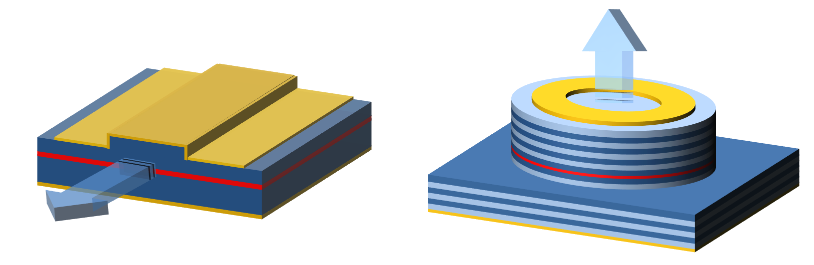
Vertical Cavity Surface Emitting Laser diodes (VCSELs) are semiconductor devices with light emission perpendicular to the chip surface. This is in contrast to the conventional edge-emitting semiconductor lasers with light emission in the plane of the chip. A schematic of the two basic laser principles is shown in Fig. 1.
Fig. 1: Principal structure of edge-emitting laser diodes (left) and VCSELs (right).
VCSELs are highly attractive for applications in optoelectronics, since they offer several advantages compared to edge-emitting (in-plane) laser diodes, such as:
low electric power consumption,
capability of on-wafer testing,
simplified fiber coupling and packaging,
longitudinal single-mode emission spectrum, and
suitability for 2D-array integration
low-cost production potential.
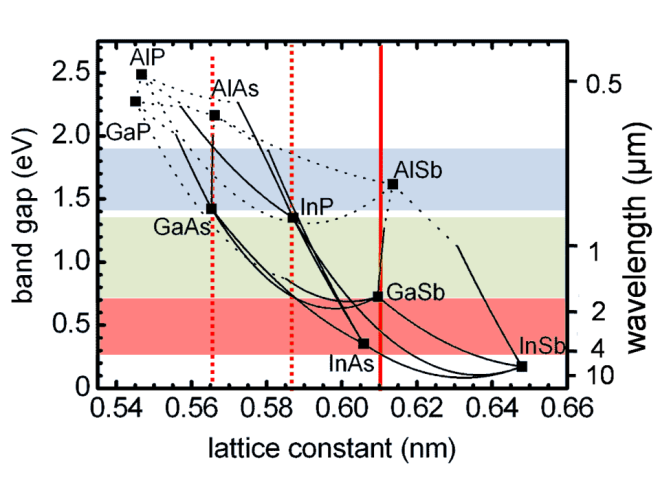
In the past, GaAs-based VCSELs in the near infrared (<1.0µm) have been developed into commercial products that are widely applied in consumer applications such as optical mice. While edge-emitting lasers for optical communications at 1.3µm and 1.55µm are well-established for a long time, the development of their VCSEL counterparts was delayed by more than a decade because of significant technological challenges related to the required material systems, such as InGaAsP/InP and AlGaInAs/InP used for 1.3- 2.3µm wavelength and AlGaInAsP/GaSb applied for 2.1µm-4µm, respectively. The relevant material systems are shown in Fig. 2, where the blue, green and red areas indicate wavelength regimes accessible by lattice-matched compound semiconductors on GaAs-, InP- and GaSb-substrates, respectively. The challenges of the InP- and GaSb-based materials required for the longer wavelengths are in particular:
Low refractive index-contrast of Distributed Bragg Reflector (DBR) mirrors
Poor thermal conductivity of ternary- (quaternary-) compound semiconductor DBRs
Large nonradiative recombination (Auger effect)
Strong degradation of optical gain performance at elevated temperatures
Selective oxidation (such as that of AlAs for the GaAs-based NIR VCSELs) for photon and current confinement not applicable
Fig.2: Bandgap energy and wavelength vs. lattice constant of GaAs-, InP- and GaSb-based compound semiconductors.
It should be noted, that by application of strained quantum wells in the active regions, the accessible wavelength ranges can be extended significantly into the long wavelength range. So, for instance, GaAs-based strained InGaAs quantum well lasers were shown up to about 1.3µm, and strained AlGaInAs quantum well lasers on InP achieve more than 2 µm emission wavelength.
Key paper:
M.-C. Amann and M. Ortsiefer, phys. stat. sol. A 1033538 (2006)
VCSEL Structure
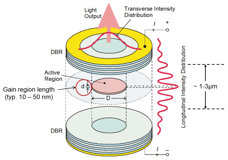
Basically, VCSELs are relatively small lasers with typical resonator dimensions of the order of a couple of wavelengths. They are therefore often called nanolasers. The principal VCSEL structure is shown in Fig.3 together with relevant dimensions.
Fig. 3: Principal structure of a VCSEL.
As can be seen, in a VCSEL the thickness of the active region d represents the length of the gain region. Differing from the edge emitters, where the laser length of typically several hundred microns corresponds to the gain region length, d is typically only of the order 10-50nm, i. e. the thickness of a multi-quantum-well structure with 1 to 8 quantum wells. Accordingly, the optical gain necessary to compensate mirror and absorption losses must be achieved over a length about four orders of magnitude shorter than in an edge emitter. Note that even edge-emitting laser diodes belong to the shortest lasers known so far. Fig. 3 also shows that the cavity length is of the order 1 to 3 µm corresponding to a few wavelengths in the semiconductor material (refractive index ~ 3 - 4). A consequence of the short cavity is a large longitudinal mode spacing which in turn leads to inherent single longitudinal mode operation of typical VCSELs. The small VCSEL geometry also results in very small threshold currents of typically 1 mA, while smallest threshold currents achievable with small VCSELs are of the order of only 10µA. Because of the short gain region length d, the VCSEL gain is rather small so that very high mirror reflectivity is required. This is usually accomplished by multilayer Bragg reflectors with reflectivities of 99% or even more made of pairs of alternating semiconductors or dielectrics with different refractive indices.
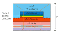
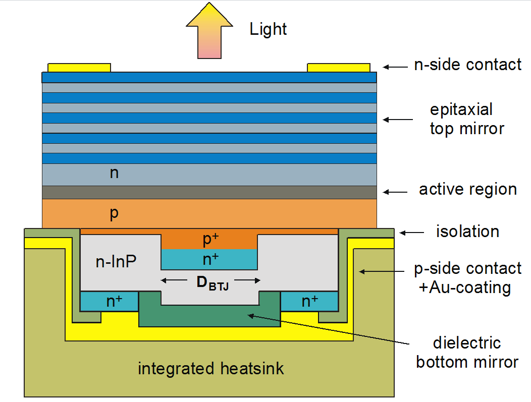
Fig.4: Principal cross-section of the buried tunnel junction in AlGaInAs/InP material system.
While short-wavelength VCSELs based on GaAs-AlGaAs are usually made with lateral photon and current confinement via steam-oxidized Al(Ga)As, other technologies have to be applied for InP- and GaSb-based long-wavelength devices. Particularly to overcome the obstacles of these materials listed in the introduction, the device concept of VCSELs with a Buried Tunnel Junction (BTJ) in conjunction with a dielectric DBR has been developed at the WSI. The functional principle of BTJs is shown in Fig. 4. A heavily p+/n+ doped layer-pair of low-bandgap material is prepared by Molecular Beam Epitaxy (MBE). It provides an ohmic-type tunnel interface that translates a current from high-resistive p-doped to low-resistive n-doped material, which substantially reduces heat generation in the device. Then, a circular or elliptic mesa is formed in a Reactive Ion Etching (RIE) process and regrown ('buried') in a second epitaxy run with n-doped InP. If a voltage is applied as indicated, the n/p+ junction aside the rest of the tunnel junction has reverse bias and therefore blocks the electrical current, which instead goes through the BTJ. This mechanism confines the current to the active region of the device, which is essential for proper VCSEL operation. Since the tunnel interface sheet resistance is as low as 3x10⁻⁶ Ωcm2, which is competitive to advanced p-side metal contacts, the voltage drop is negligible.
Fig.5: Complete VCSEL structure.
Due to the integration of the BTJ, the VCSELs are slightly thicker at the center (ΔL / Leff >> 1%) wherefore the boundary conditions of the optical field yield an efficient wave-guiding that is of comparable magnitude to that of steam-oxidized GaAs-based VCSELs. The optical and the electrical guidance by the BTJ are conveniently self-aligned. In the complete BTJ-VCSEL structure (Fig. 5) the BTJ is found upside down, and the InP substrate is totally removed. The active region where the light is generated is placed above the BTJ. For a λ=1.55µm device, it comprises five 8nm thick compressively strained InGaAlAs quantum wells. The front side mirror atop the active region is an epitaxial DBR with about 35 layer-pairs of InGaAlAs/InAlAs yielding a calculated power reflectivity of 99.4%. The back side mirror consists of a dielectric layer stack as a DBR in conjunction with a gold termination that boosts the reflectivity to approximately 99.75%. Because of the higher refractive index contrast of the dielectric materials (e.g. amorphous CaF2/Si for λ=1.55µm),the dielectric DBR is significantly thinner compared to an equivalent InP-based semiconductor DBR and has a smaller thermal resistance, even though the resistivity of the dielectric materials can be higher. This is important for the heat sinking in the Laser. For example, a device with a BTJ diameter DBTJ of 10µm enabling a dielectric back reflector could have a thermal resistance of 3000 K/W Instead of 8000 K/W with an equivalent InP-based semiconductor DBR.
Current is injected through the integrated heat sink of electroplated gold (+) and a gold pad on the top. It can be seen that except for a thin layer of ~100nm (marked red in Fig. 5) the whole current path is n-doped. This is especially important for the current injection laterally around the dielectric material where a p-doping would cause too much heat.
VCSELs for communications at 1.3-1.55µm wavelength
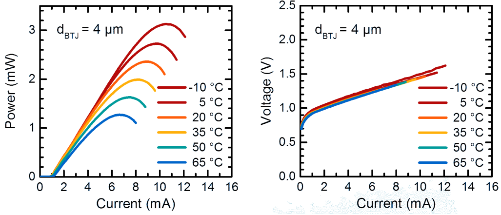
Continuous-wave (cw) Power-current and voltage-current characteristics of a 1.3µm VCSEL with circular BTJ of 4µm diameter are shown in Fig. 7 over the temperature range of -10°C to 65°C. It features a single-mode output power of 3mW, which is the highest reported output power for electrically pumped single-mode long-wavelength VCSELs. At the threshold current of about 1mA, the voltage drop is just about 0.95V, and due to a low series resistance of 50 Ohms, the operation voltage at 3mW is still below 1.5V. While the output power decreases with operation temperature down to about 1.2mW at 65°C, the threshold current is almost temperature independent. The latter is achieved by a negative ‘detuning’ of the gain peak wavelength against cavity resonance at lower temperatures, i. e. the gainpeak is at lower wavelength than the lasing wavelength at low temperatures. Due to the ~5 times larger temperature coefficient of the gain peak wavelength relative to the cavity resonance, the detuning decreases with temperature and thus improves the gain at the lasing wavelength so that the strong temperature dependence of the active region gain can be compensated over a certain temperature range.
Fig.6: Optical output power and driving voltage vs current of a 1.3µm single-mode VCSEL.
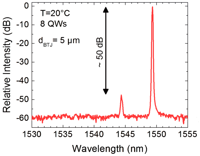
The BTJ-VCSELs are usually excellent single-mode emitters with a strong suppression of side modes by more than three orders of magnitude. A typical spectrum of a 1.55µm VCSEL is shown in Fig. 8 indicating a suppression of the next-order mode at ~1.545µm by some 50 dB (five orders of magnitude).
Fig.7: Temperature characteristics of BTJ-VCSELs at 1.55µm wavelength.
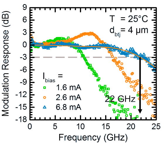
For communications applications at 1.3µm – 1.55µm the modulation bandwidth is of paramount importance. First, the analogue small-signal modulation response of a high-speed 1.55µm VCSEL is shown in Fig. 9. As can be seen, with increasing bias current, the 3dB cutoff-wavelength increases (according to theory) up to more than 20 GHz. Due to strong damping, there is only a weak resonance peak. This makes these lasers very well suited for large-bandwidth analog and digital communication systems.
Fig.8: Small-signal analogue modulation response of BTJ-VCSEL at 1.55µm wavelength. The threshold current is around 1mA.
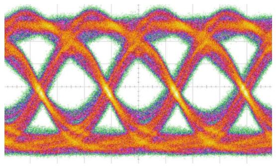
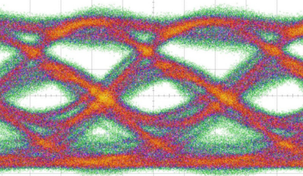
The digital modulation performance of a laser is usually investigated by the eye-diagrams taken at increasing bit rates, where the eye opening indicates the ability to distinguish between a logical 0 or 1 and, thus, the suitability for operation at this bit rate. For the same laser, the corresponding eye diagrams at ultra-high bit rates of 40Gb/s and 50Gb/s are shown in Fig 10.
Fig.9: Eye diagrams of BTJ-VCSEL at 1.55µm wavelength at bit rates of 40Gb/s (left) and 50Gb/s (right), respectively. The time axis scaling is 10ps/div..
As can be seen, excellent eye openings are achieved at 40 Gb/s and even at 50Gb/s sufficient bit error rates can be obtained with proper error correction techniques. In fact, 56 Gb/s have been demonstrated with these lasers in a transmission experiment together with Bell Labs.
The concept of long-wavelength VCSELs in the (InGaAl)As/InP material system employing a BTJ has proved suitability even for a wavelength range from 1.3µm to 2.3µm. Moreover, excellent threshold performance is achieved with 1.83µm-VCSELs, such as output powers exceeding 1mW with large devices and threshold currents as low as 190µA. Lasing activity in cw-mode operation has been demonstrated to sustain up to 90°C. These properties can be attributed to a relatively high index step in the InGaAs/InAlAs epitaxial front DBR, strongly strained InGaAs quantum wells in the active region, and a high-reflective Al2O3/Si back DBR with practically no optical absorption.
Key papers:
C. Xie et al., J. Lightwave Technol. 33670 (2015)
S. Spiga et al., J. Lightwave Technol. 35727 (2016)
GaSb-based VCSELs for sensing applications in the 3µm to 4µm wavelength range
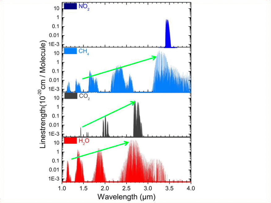
A highly encouraging application for VCSELs is the monitoring of trace gases such as CH4, HCN, H2O, HCl, N2O, CO, and CO2, which have typical absorption lines in the infrared. A compilation of the absorption lines of several interesting gases is given in Fig. 11. As can be seen, a characteristic behavior is the strong increase of line strength with increasing wavelength. For instance, the line strength of methane (CH4) increases by about three orders of magnitude by raising the wavelength from ~1.1µ to 3.3µm. Accordingly, wavelengths in the mid-infrared (>3µm) are of major importance for this application. Of course, laser sources must be single-mode and continuously tunable to be suited for this so-called TDLAS (Tunable Diode Laser Absorption Spectroscopy).
Fig.10: Wavelength-dependent absorption lines of several gases at room temperature and normal pressure.
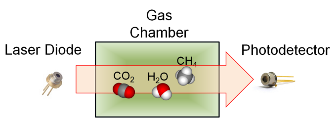
To determine the types of gases and their concentration, the electrical current through a single-mode VCSEL is modulated, the inner temperature of the VCSEL follows, and so does the emission wavelength. Tuning ranges of more than 5nm are achievable. The laser beam travels through a probe chamber with the gas mixture to analyze and the transmitted light intensity is measured by a detector (Fig. 12). Then, the relative intensity loss compared to the evacuated chamber is computed. Since this simple yet efficient and fast-response method requires less than 1mW of laser power, VCSELs are the light sources of choice due to low power consumption, low price and eye-safety reasons.
Fig.11: Setup for trace gas sensing with single-mode lasers.
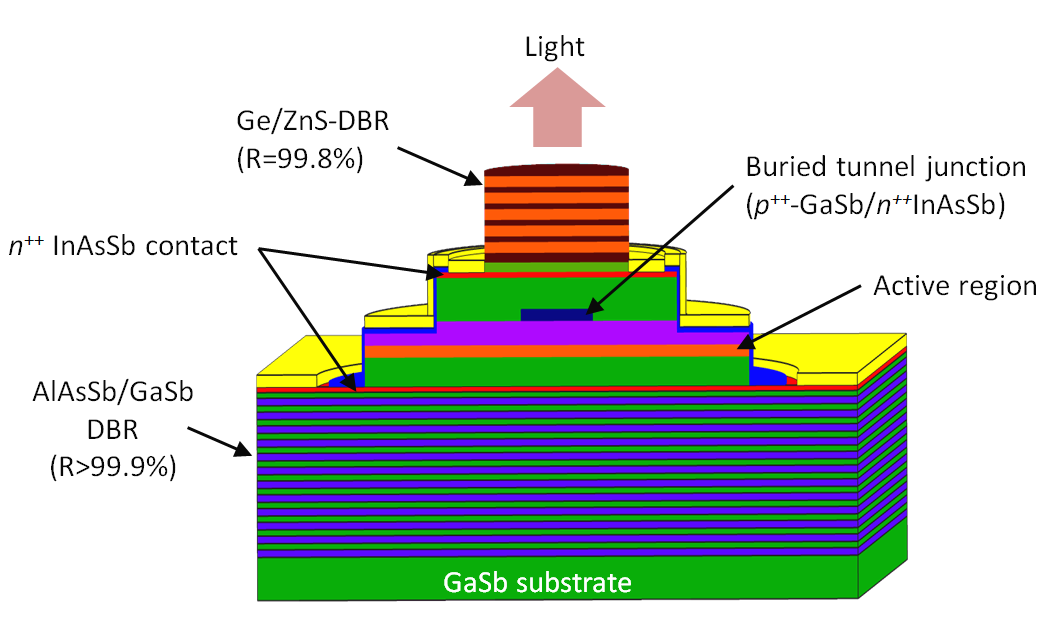
As mid-infrared laser sources are preferred, VCSELs based on GaSb are required that have covered so far the 2.7µm – 4µm wavelength range. The principal structure of a GaSb-based BTJ-VCSEL is displayed in Fig. 13.
Fig.12: Principal device structure of GaSb-based BTJ-VCSELs for the 2.7-4µm wavelength range.
Differing from the InP-based counterparts, the GaSb-VCSELs are made in an up-side-up configuration with the heat sinking via the epitactic DBR and the substrate. This is because the thermal conductivity of the DBRs in the GaSb material system is much better than in the InP-based AlGaInAs materials. Also, because of the strong enhancement of free-carrier absorption with increasing wavelength (Drude model: absorption ~ 2), an undoped epitactic DBR is used together with intracavity n++-doped InAsSb contact layers. These are placed in nodes of the electromagnetic field so that their absorption losses can completely be neglected.
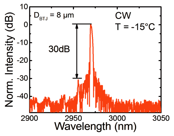
As with the InP-based BTJ-VCSELs decent single-mode lasing has been achieved at all wavelengths. Fig. 14 shows a typical emission spectrum of a 3µm device exhibiting some 30dB side mode suppression ratio.
Fig.13: Emission spectrum of a 3µm GaSb-based BTJ-VCSEL with an aperture diameter of 8µm operated at -15°C.
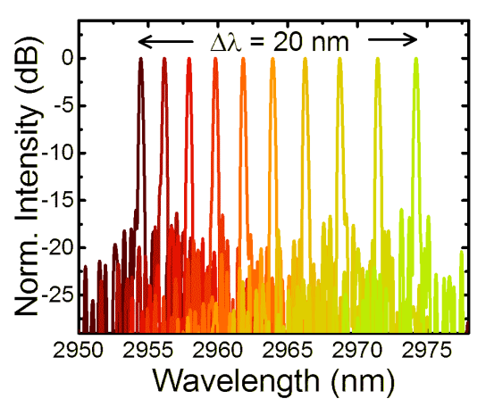
As continuous wavelength tenability is of major relevance in TDLAS, the electro-thermal wavelength tuning of VCSELs can be accomplished. This technique is extremely simple because only the laser current must be varied yielding a continuous wavelength shift. The corresponding tuning behavior of the 3µm VCSELs is presented in Fig. 14 showing a considerable continuous tuning range of 20 nm.
Fig.14: Tuning spectra of a 3µm GaSb-based BTJ-VCSEL obtained by varying the laser current
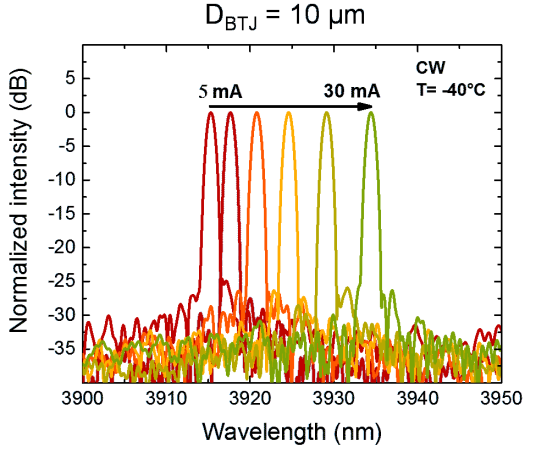
Recently, GaSb-based VCSELs with type-II heterostructure active regions were realized up to 4µm wavelength, where a continuous-wave lasing can be achieved up to 7°C. The 4µm lasers also yield excellent single-mode performance and decent tuning behavior with again some 20nm tuning range as illustrated in Fig. 15.
Fig.15: Current tuning spectra of a 4µm GaSb-based BTJ-VCSEL with a 10µm wide aperture.
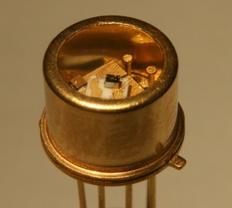
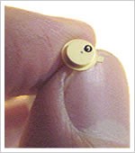
For the TDLAS application, the lasers are usually mounted on a temperature-controlled housing so that operation temperatures down to less than 0°C are possible. A corresponding laser in a TO housing with integrated Peltier cooler is shown in Fig 15 together with a laser mounted without integrated Peltier element.
Fig.16: Tunable VCSEL mounted on a TO-housing with (left) and without (right) integrated Peltier element for cooling and temperature control.
Key papers:
Andrejew et al., Opt. Lett. 412799 (2016)
G. Veerabathran et al., Appl. Phys. Lett. 110071104 (2017)
Quantum Cascade Lasers for the Mid- to Far-Infrared Spectral Region
Classical concept of quantum-cascade lasers
A quantum-cascade (QC) laser is based on intersubband-transitions of electrons inside a quantum-well structure. Therefore, unlike other semiconductor light sources, the emitted wavelength is not determined by the band gap of the used material but on the thickness of the constituent layers.
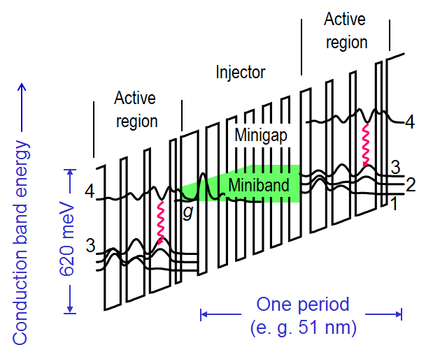
Fig. 1: Typical structure of a quantum-cascade laser.
The classical concept of QC lasers is a periodic repetition of active sections and so-called injector regions, in which a miniband is formed. A typical structure is shown in Fig. 1. From the injector miniband the electrons are injected into the upper laser energy level (4) of the active section. Here the laser transition takes place. After that, the lower laser energy level (3) is emptied by LO-phonon emissions and the electrons enter the next stage by tunnelling.
Quantum-cascade lasers without injector regions
Injector regions have been considered as an essential requirement for laser action in QC lasers. In the active sections the photons are generated, while the miniband in the injector regions enables the transfer of the electrons from the lower levels of one active section into the upper level of the next section. Due to the doping of these regions, they act as an electron reservoir and provide stable current flow. Furthermore, the injector miniband helps to avoid a thermal backfilling of the lower laser level. However, apart from these benefits, the main disadvantage of these structures is the lengthening of the active stage with optically passive and slightly absorbing material and therefore a reduced overlap of the waveguide mode with the active sections. QC lasers without injector regions are expected to yield improved performance, provided that problems like thermal backfilling can be avoided and the electron transfer can be managed otherwise.
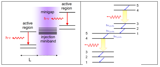
Fig. 2: Concept of a conventional (left) and an injectorless (right) QC laser, based on a five-level staircase.
The concept of our QC laser without injector miniband is based on a five-level staircase (Fig.2). At a certain bias field, levels 1 and 2 of one active section are resonant with levels 4 and 5 of the following section and a double LO-phonon resonant condition occurs. Therefore, after the radiative transition (between levels 4 and 3), the electrons are transferred directly from one active section into the next, without the need for a bridging miniband. The bias field can be increased until level 1 is brought into resonance with level 5 and a triple LO-Phonon condition is realized. Thus, a thermal backfilling of the lower laser level can be avoided.
Active region design and laser performance
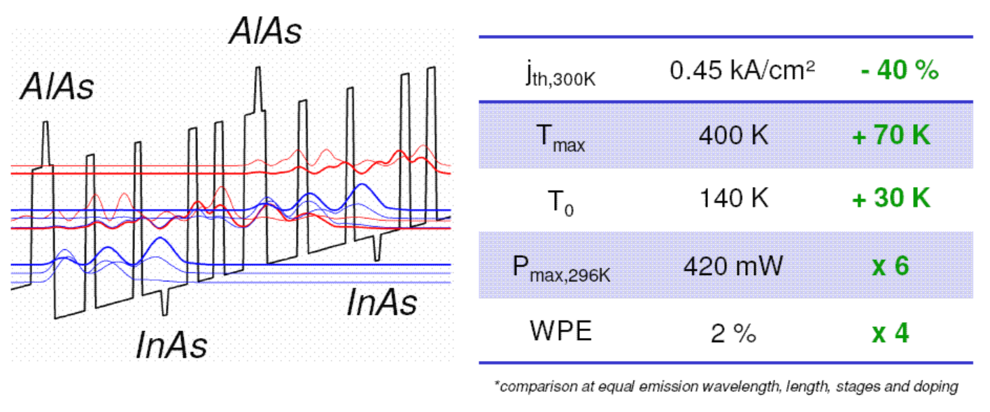
Most quantum cascade laser (QCL) designs use only two different material compositions. One material composition (i. e. GaInAs or GaAs) is used as the well and the other (i. e. AlInAs or AlGaAs ) is used as the barrier. In our group, we have implemented high bandgap AlAs into the barrier to suppress carrier escape into the continuum. Additionally, we included thin layers of InAs into the transition well for increased dipole matrix element and carrier lifetime in the upper state. Fig. 3 illustrates the schematic band diagram of the device with four material compositions, which demonstrated record low threshold current densities at room temperature in pulsed operation mode. The device is emitting around 7 µm.
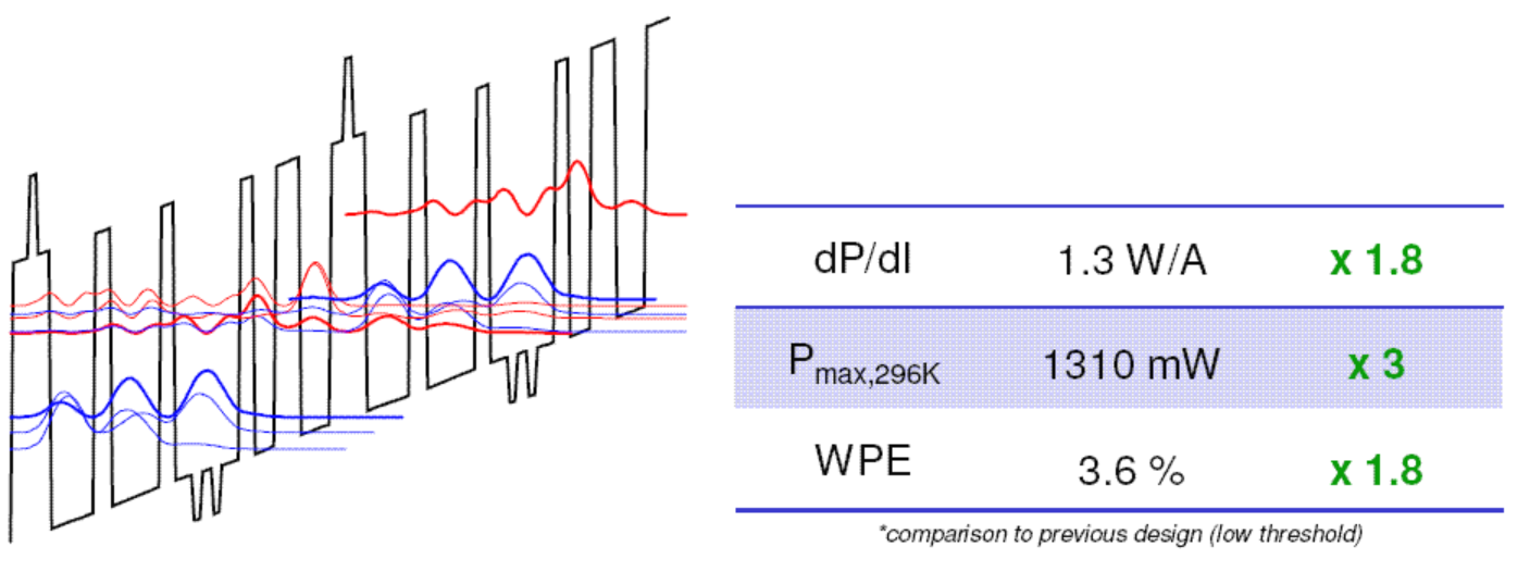
Fig. 4 illustrates the conduction band profile for the mid infrared device with two InAs layers in the transition well. The device had an emission wavelength of 5.6 µm and optical output power of 1.3 W with a slope efficiency of 1.3 W/A at room temperature in pulsed operation.
Fig.3: Conduction band profile and wavefunctions (left) at a bias field of 103 kV/cm for the four material based mid infrared QCL. Device parameters and improvement to conventional design are given in the table (right). (WPE: wall plug efficiency).
Fig.4: Conduction band profile and wavefunctions (left) at a bias field of 127 kV/cm for the four material based mid infrared QCL with two InAs layers. Device parameters and improvement to conventional design are given in the table (right). (WPE: wall plug efficiency).
Far-Infrared Quantum Cascade Lasers by intracavity nonlinear frequency mixing
Device Concept
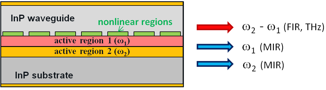
It has been demonstrated that intersubband transitions in quantum wells can be tuned to exhibit a giant second-order ((2)) nonlinear optical response, which yields resonant properties. Such synthetic nonlinearities can be monolithically integrated with a dual-wavelength Mid-IR QCL as shown in Fig. 5. These integrated lasers represent efficient nonlinear radiation sources with a spectral coverage in the Near-IR (2 - 4 µm) by sum-frequency generation, and in the Far-IR (15 - 200 µm) by difference frequency generation, respectively. Commonly because of the corresponding frequencies, the Far-Infrared range is also denoted as THz regime.
Fig. 5: Schematic longitudinal section of an integrated nonlinear QCL for THz emission via difference frequency generation in a quasi-phase-matched configuration as accomplished by a grating.
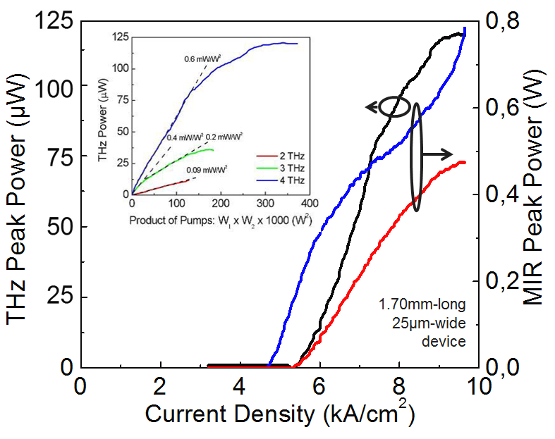
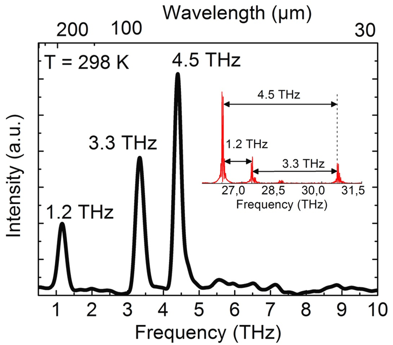
On this subject, we work in a close collaboration with Prof. M. A. Belkin's group at the University of Texas at Austin. Our research areas include development of room-temperature operating devices in the Near-IR by intracavity quasi-phase-matched second-harmonic-generation and terahertz devices by difference-frequency-generation. Our research breakthroughs include room-temperature lasing in AlInAs/GaInAs/InP based devices down to 2.7 µm by second-harmonic generation, and 210 K lasing at 70 µm wavelength by difference-frequency-generation (DFG) (Figs. 6 and 7).
Fig.6: Room-temperature MIR and THz light-output vs. current density data for a device emitting around 70 µm. Emission spectrum of the pump and the nonlinear signals can be seen in the inset.
Fig.7: Difference-frequency signal (~70 µm) at 78 K and 210 K of the device in Fig. 6. The corresponding pump emission spectrum is shown in the inset. Because of multimode operation more than two MIR peaks are observed.
Quantum Cascade Laser Device Technology
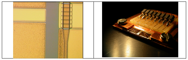
Our QCL structures are grown by solid source molecular beam epitaxy (SS-MBE). The epitaxial structures are then processed in our class 100 cleanroom environment. The process involves optical lithography, dry-etching, wet-chemical etching, dielectric deposition via PECVD or sputtering. For contacts, e-beam evaporation in ultra-high vacuum environment is used. Additional Au electroplating is applied for improved heatsinking purposes. When needed, re-growth is performed in MOVPE. A top view of the nonlinear THz and a photgraph of a mounted laser bar with several QCLs are displayed in Fig 8.
Fig.8: Top optical microscope image of a THz-DFG device and photograph of QCLs mounted on a copper heat sink.

 Walter Schottky Institut